News Brief
Rs 76,000cr Boost To Semiconductor Manufacturing In India; Global Chip Companies Setting Up Fabs In India Will Get Up To 50% Of Project Cost As Government Subsidy
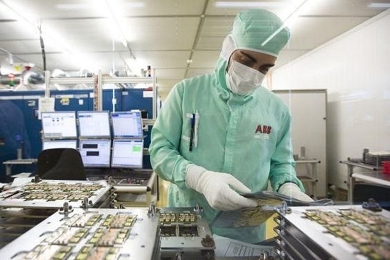
A semiconductor plant in India. (Representative image)
In a pathbreaking move that aims to propel India as a hub for electronics, the Modi government plans today approved a IN₹76000 crores (approximately $10 billion) incentive package towards setting up over 20 semiconductor designs, components manufacturing, and display fabrication (fab) units over the next six years.
The government said that the incentive package for semiconductor ecosystem will help usher in a new era in electronics manufacturing by providing a globally competitive incentive package to companies in semiconductors and display manufacturing as well as design.
With the approval of the programme for development of semiconductors and display manufacturing ecosystem in India with an outlay of Rs.76,000 crore $10 billion), Government of India has announced incentives for every part of supply chain including electronic components, sub-assemblies, and finished goods.
Incentive support to the tune of Rs.55,392 crore ($7.5 billion) have been approved under PLI for Larges Scale Electronics Manufacturing, PLI for IT Hardware, SPECS Scheme and Modified Electronics Manufacturing Clusters (EMC 2.0) Scheme. In addition, PLI incentives to the quantum of Rs.98,000 crore ($13 billion) are approved for allied sectors comprising of ACC battery, auto components, telecom & networking products, solar PV modules and white goods.
The incentives approved by the Modi government for the development of semiconductors and display manufacturing ecosystem in India includes
The union government will work closely with the state governments to establish high-tech clusters with requisite infrastructure in terms of land, semiconductor grade water, high quality power, logistics and research ecosystem in order to establish atleast two greenfield Semiconductor Fabs and two Display Fabs in the country.
Semi-conductor Laboratory (SCL): Union Cabinet also approved a proposal for modernization and commercialization of Semi-conductor Laboratory (SCL). The Ministry of Electronics and Information Technology (MeitY) will explore the possibility for the Joint Venture of SCL with a commercial fab partner to modernize the brownfield fab facility.
Compound Semiconductors / Silicon Photonics / Sensors (including MEMS) Fabs and Semiconductor ATMP / OSAT Units: The Scheme for Setting up of Compound Semiconductors / Silicon Photonics / Sensors (including MEMS) Fabs and Semiconductor ATMP / OSAT facilities in India shall extend fiscal support of 30% of capital expenditure to approved units. Atleast 15 such units of Compound Semiconductors and Semiconductor Packaging are expected to be established with Government support under this scheme.
Semiconductor Design Companies: The Design Linked Incentive (DLI) Scheme shall extend product design linked incentive of up to 50% of eligible expenditure and product deployment linked incentive of 6% - 4% on net sales for five years. Support will be provided to 100 domestic companies of semiconductor design for Integrated Circuits (ICs), Chipsets, System on Chips (SoCs), Systems & IP Cores and semiconductor linked design and facilitating the growth of not less than 20 such companies which can achieve turnover of more than Rs.1500 crore in the coming five years.
Introducing ElectionsHQ + 50 Ground Reports Project
The 2024 elections might seem easy to guess, but there are some important questions that shouldn't be missed.
Do freebies still sway voters? Do people prioritise infrastructure when voting? How will Punjab vote?
The answers to these questions provide great insights into where we, as a country, are headed in the years to come.
Swarajya is starting a project with an aim to do 50 solid ground stories and a smart commentary service on WhatsApp, a one-of-a-kind. We'd love your support during this election season.
Click below to contribute.
Latest