Technology
India’s Semiconductor Efforts Get A Shot In The Arm With Launch Of Chipmaker AMD’s Largest Global Design Centre In Bengaluru
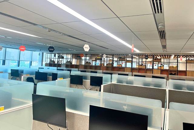
A glimpse at the new AMD Bengaluru campus workspace.
Under partly cloudy skies, the mood was contrastingly sunny under the roof of Prestige Technostar in east Bengaluru on Tuesday (28 November).
The California-based chipmaker Advanced Micro Devices (AMD) kicked off its largest design centre worldwide in Bengaluru, near the technology nerve centre of Whitefield, on 28 November.
The launch of this research-and-development campus is an accomplishment of a significant chunk of AMD’s India growth plan — revealed exactly three months ago at the Semicon India 2023 conclave in Gandhinagar, Gujarat — which entails an investment in India of approximately $400 million over the next five years.
According to AMD, the new campus, which already makes up about a quarter of that planned investment in the country, marks “a milestone in the company's commitment to expand research, development, and engineering operations in India.”
Impressively, the facility stands as the largest investment made by AMD in facilities anywhere in the world.
The Tuesday launch signals the completion of phase one, with phase two set to be wrapped up by the third quarter of 2024.
The 50,000-square-foot design centre was inaugurated by Ashwini Vaishnaw, the Union Cabinet Minister for Railways, Telecommunications, and Electronics and Information Technology in the Government of India.
The Narendra Modi government has been dogged in their drive to build semiconductor muscle within India, and Vaishnaw has been at the forefront of implementing this vision.
“AMD setting up its largest design centre in Bengaluru is a testament to the confidence global companies have in India,” the Minister said.
The AMD Technostar campus will see, by the end of 2028, about 3,000 AMD engineers working together to design and develop semiconductor technology, including 3D stacking, artificial intelligence, and machine learning.
This new workforce will be over and above the more than 7,000 AMDers already working in India today, built from the ground up since the initiation of the company's India journey in 2001 with only a handful of employees.
Cut to 2023, AMD’s India employees constitute about 25 per cent of the semiconductor design company’s global workforce.
The new AMD joinees will help advance AMD’s cause of high-performance computing. “The campus will serve as a centre of excellence for the development of leadership products across high-performance CPUs for the data center and PCs, data center and gaming GPUs, and adaptive SoCs and FPGAs for embedded devices,” AMD has said.
The facility will broadly achieve a couple of objectives for India — move the needle on building a world-class semiconductor design and innovation ecosystem in India and provide opportunities for the country's large pool of skilled semiconductor engineers.
Further, as Rajeev Chandrasekhar, the Minister of State for Electronics and Information Technology, Skill Development and Entrepreneurship, said following AMD’s investment announcement in July, it “will catalyse PM Narendra Modi’s vision of India becoming a global talent hub.”
As for AMD, India presents a huge opportunity in terms of semiconductor talent and expansion of high-performance work.
According to the Semiconductor Industry Association, one in five semiconductor design jobs is in India. A large centre of the kind now launched in Bengaluru enables the tapping of India’s proliferating engineering talent.
With about two decades of experience in India, AMD also finds a stable ground from which to build further in the country.
Moreover, India, with its vast semiconductor potential, offers multinational chip companies the opportunity to diversify their supply chains — particularly away from China — as appears to be the larger trend in the industry at present.
At the inauguration ceremony, Vaishnaw was accompanied by top AMD leaders. Among the AMD leadership team present were Mark Papermaster, Executive Vice President and Chief Technology Officer; Jaya Jagadish, India Country Head; and Deepak Agarwal, Bengaluru Site Lead.
Jagadish in particular is well versed with India’s overall semiconductor efforts, having served previously as the chairperson of the Semicon Talent Building Committee under India Semiconductor Mission.
The new Bengaluru facility, she said, marks “the next milestone in our (AMD’s) growth journey to be a significant contributor in the advancement of semiconductors.”
For Papermaster, establishing AMD’s largest global design centre in Bengaluru “showcases our (AMD’s) confidence in the exceptional engineering talent that the country has to offer.”
“This new design center will help propel technology and product development across the AMD portfolio, fueling the next generation of high performance, adaptive and AI computing solutions for our customers around the world,” he said.
Speaking at Semicon India 2023 earlier this year, Papermaster said, “By further investing and expanding our presence in Bangalore, we are committed to driving innovation in India to support the India Semiconductor Mission.”
As for the “extremely proud” site lead Agarwal, the Technostar campus is more than just a state-of-the-art building. “It is the embodiment of our mission to build great products that accelerate next generation computing experiences.”
“The campus will provide a great workspace for our India teams to be creative and innovative in their pursuit to support the company’s growth as a high performance and adaptive computing leader,” added Agarwal.
The campus architecture is inspired by Indian heritage. The workspace is designed with the aim of fostering creativity and collaboration. Given that it's primarily an research-and-development facility, various labs spread out across a 60,000-square-foot area. A "patent wall" puts on display AMD innovation.
The campus also includes a cafeteria acoustically engineered to host gatherings of more than 2,000 employees, as well as a gym and a yoga centre to promote the holistic health and well-being of AMD employees, AMD said.
The choice of location for the new AMD campus was influenced by two factors. Agarwal told reporters that about 60-65 per cent of their employees were based around the Whitefield area and would, perhaps, as a result, be comfortable working close by at this campus.
Further, the location presents AMD India with potential for further expansion at a later stage, even beyond 2028, the year until when the planned investment has been announced.
AMD has been an innovator in high-performance computing, graphics, and visualisation technologies for more than five decades. It took off in India in 2001 with the launch of the first site in New Delhi.
With the inauguration of the new Bengaluru campus, the AMD India office footprint has now risen to 10 locations across the cities of Bengaluru, Delhi, Gurugram, Hyderabad, and Mumbai.
Support Swarajya's 50 Ground Reports Project & Sponsor A Story
Every general election Swarajya does a 50 ground reports project.
Aimed only at serious readers and those who appreciate the nuances of political undercurrents, the project provides a sense of India's electoral landscape. As you know, these reports are produced after considerable investment of travel, time and effort on the ground.
This time too we've kicked off the project in style and have covered over 30 constituencies already. If you're someone who appreciates such work and have enjoyed our coverage please consider sponsoring a ground report for just Rs 2999 to Rs 19,999 - it goes a long way in helping us produce more quality reportage.
You can also back this project by becoming a subscriber for as little as Rs 999 - so do click on this links and choose a plan that suits you and back us.
Click below to contribute.
Latest