Science
Indian Scientists Develop Super Flexible Composite Semiconductor For Next-Gen Displays And Wearables
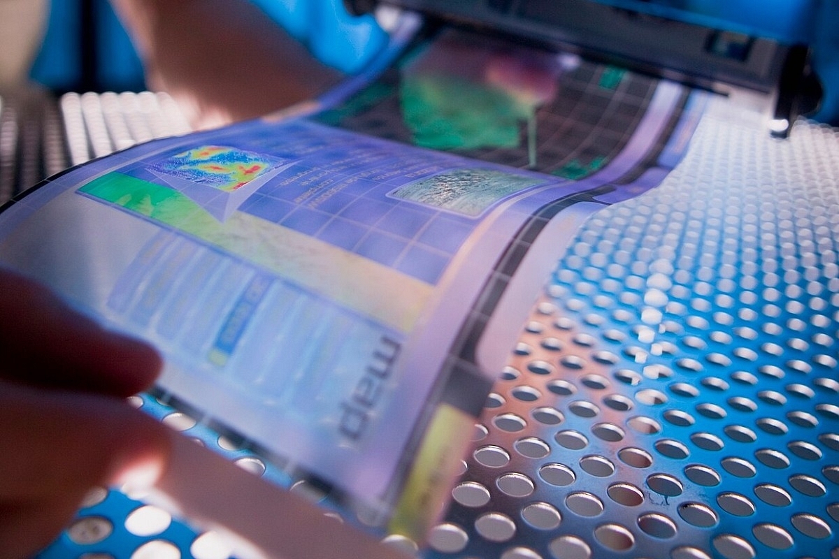
Representative Image (Pic Via Wikipedia)
Scientists at the Indian Institute of Science (IISc) have developed a composite semiconductor material that is super flexible.
This material has the potential to be used in next-generation flexible or curved displays, foldable phones, and wearable electronics.
Traditional semiconductor devices, such as transistors, which are the building blocks of most electronic circuits used in the display industry, are typically made of amorphous silicon or amorphous oxides.
However, both of these materials are not flexible or strain tolerant. Although adding polymers to oxide semiconductors can increase their flexibility, there is a limit to how much can be added without compromising the performance of the semiconductor, according to IISc.
In a recent study published in the journal 'Advanced Materials Technologies', researchers from the Department of Materials Engineering at IISc have discovered a way to fabricate a composite material that contains a significant amount of polymer.
This composite can contain up to 40 per cent of the material weight in Polymer and is produced using a solution-process technique called inkjet printing.
Previous studies have only reported polymer additions of up to one to two percent.
Interestingly, the addition of a large quantity of polymer did not alter the semiconducting properties of the oxide semiconductor. This resulted in a highly flexible and foldable composite semiconductor without compromising its performance, the Bengaluru-based Indian Institute of Science (IISc) in said in a statement on Tuesday.
The composite semiconductor is composed of two materials: a water-insoluble polymer, such as ethyl cellulose, which provides flexibility, and indium oxide, a semiconductor that offers excellent electronic transport properties.
To create this material, the researchers mixed the polymer with the oxide precursor in a way that formed interconnected oxide nanoparticle channels.
These channels surrounded phase-separated polymer islands, allowing electrons to move from the source to the drain of a transistor, ensuring a steady current flow.
The researchers discovered that the key to forming these connected pathways was selecting the right type of water-insoluble polymer. This polymer needed to avoid mixing with the oxide lattice during the fabrication of the oxide semiconductor.
According to Subho Dasgupta, an Associate Professor in the IISc's Department of Materials Engineering and the corresponding author of the study, the process of "phase separation" and the creation of polymer-rich islands helps in crack arrest, making it super flexible,
Instead of using traditional deposition techniques like sputtering, Dasgupta's team employed inkjet printing to apply their semiconductor material onto a variety of flexible substrates, including plastics and paper.
The study utilised a polymer material called Kapton.
Just like words and images printed on paper, electronic components can be printed on any surface using special functional inks containing either electrically conducting, semiconducting or insulating materials. However, there are challenges.
Mitta Divya, the first author of the study and a former PhD student at the Department of Materials Engineering (currently a postdoc at King Abdullah University of Science and Technology), explained that achieving a continuous and uniform film can be difficult.
"Therefore, we had to optimise certain protocols, for example, preheating the printed semiconductor layer on the Kapton substrate prior to high temperature annealing," Divya said, reports NDTV.
Another challenge in printing ink is ensuring the appropriate environmental conditions. If the humidity is too low, the ink can dry up within the nozzle, making it impossible to print, said Dasgupta.
In the future, printed semiconductors could be utilised to create fully printed and flexible television screens, wearables, and large electronic billboards.
This advancement in technology could potentially revolutionise the display industry by offering low-cost and easily manufactured options, according to Dasgupta.
The team has obtained a patent for their material and plans to conduct tests on its shelf life and quality control across various devices. These tests are necessary before scaling up production for mass manufacturing. Additionally, the team intends to explore other polymers that can aid in the design of flexible semiconductors (statement).
Support Swarajya's 50 Ground Reports Project & Sponsor A Story
Every general election Swarajya does a 50 ground reports project.
Aimed only at serious readers and those who appreciate the nuances of political undercurrents, the project provides a sense of India's electoral landscape. As you know, these reports are produced after considerable investment of travel, time and effort on the ground.
This time too we've kicked off the project in style and have covered over 30 constituencies already. If you're someone who appreciates such work and have enjoyed our coverage please consider sponsoring a ground report for just Rs 2999 to Rs 19,999 - it goes a long way in helping us produce more quality reportage.
You can also back this project by becoming a subscriber for as little as Rs 999 - so do click on this links and choose a plan that suits you and back us.
Click below to contribute.
Latest