Tech
Know More About Display Fabs And AMOLED From The Technology Guide For Rajesh Exports-Owned Elest
- Grantwood Technologies is believed to be guiding Elest, a subsidiary of Rajesh Exports, which is building India's first modern display manufacturing unit in Telangana.
AMOLED displays.
With the Union government's Rs 76,000 crore incentives package for domestic manufacturing of semiconductors and displays, Elest, a subsidiary of Rajesh Exports, has decided to build India's first modern display manufacturing unit in Telangana.
There is no easily available public information on who is providing the technology knowhow to Elest. However, based on various pointers, Swarajya had reported that it is likely that a company called Grantwood Technologies could be guiding them.
In May 2021, in media reports like this which gave hints of the upcoming incentive scheme for display fabs, there is a mention of a study by the India Cellular and Electronics Association (ICEA) and Grantwood Technologies. Director and chief executive officer of Grantwood Technologies G Rajeswaran (also a Professor of Practice at IIT Madras as per his LinkedIn profile), was quoted in some of the media reports as a display expert and has played a key role in the study published by ICEA.
The nearly 50-page study titled "Flat Panel Displays — Creation of a Display Industry in India" is available on ICEA website, and gives an overview of flat display technologies and market in general and opportunities for India in particular.
As per the report, the global display market is predicted to be about $126 billion by 2024, most of which is driven by mobile phone, followed by televisions.
The cumulative Indian market demand for displays between 2021 to 2025 is likely to be $60 billion. Display fabs in India will create value-addition of greater than $11 billion annually from Year 5 and create new display export opportunities from India of up to $10 billion by Year 5.
Flat panel displays are fabricated by the integration of its building-block technologies, namely,
a) Thin film transistor (TFT) backplane,
b) Liquid crystal display (LCD) panel or organic light emitting diode (OLED) panel frontplane and,
c) The assembly of module components.
There are several technology choices within each of these building-block categories and the combination of technology choices is selected to ensure that the display can meet or exceed the technical requirements demanded by the display-centric end product.
The active matrix organic light emitting diode (AMOLED) based displays were first demonstrated in 1999 by the combination of TFT backplanes used in TFT-LCD displays and OLED devices deposited over them. They entered mass-production in 2002 and were first commercialised in 2003 for digital still camera and mobile phone applications. The first AMOLED displays for use in TVs was developed in 2006 and introduced to the market in 2012.
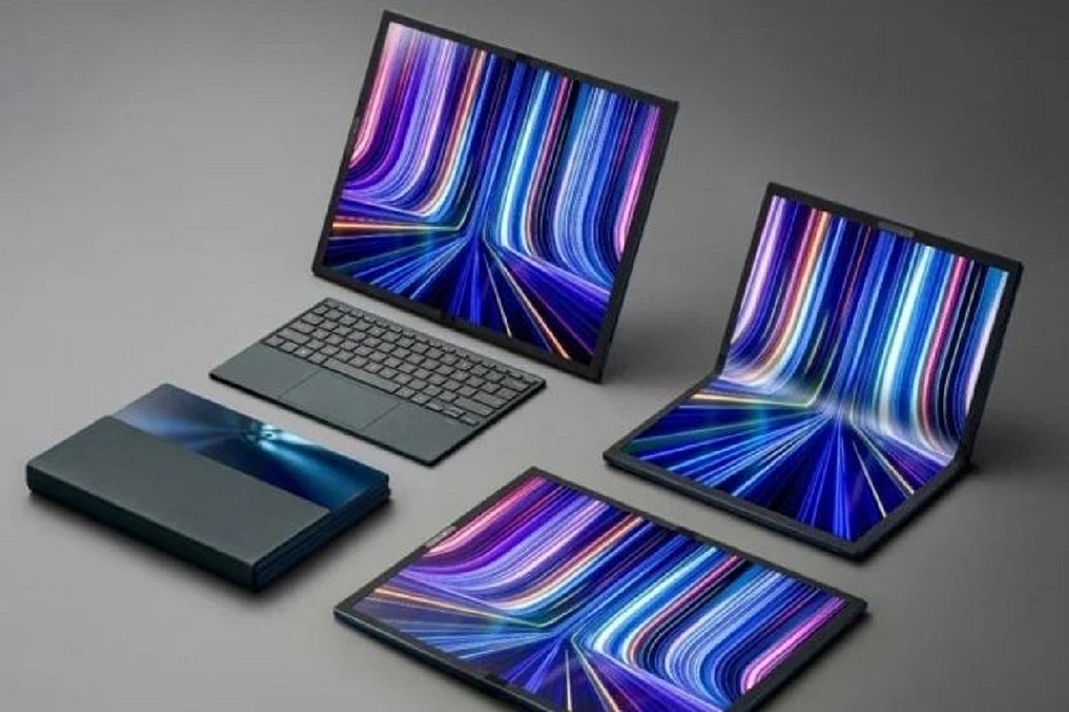
As AMOLED display production costs decreased with increasing production experience, they started eroding the market share of equivalent LCD displays in smartphone applications. The development and emergence of flexible AMOLED display technology that allows bendable, foldable and rollable display-centric product designs provides another vector of new growth opportunity.
Flexible display products are likely to contain foldable or rollable AMOLED displays in the future. Two of the major display manufacturers (Samsung and LG Display) have already announced their intention to focus all their future development and manufacturing on AMOLED displays and stop further development activities in TFT-LCD products, as the enabling display attribute of flexibility is only available with AMOLED displays.
The display manufacturing supply chain consists of suppliers of patterning materials, functional materials, optical materials, process equipment, metrology tools, subcomponents for module assembly, display driver ICs, factory automation, cleanroom and auxiliary equipment either for LCD or AMOLED display production.
The bill of materials (BoM) for of LCD display assembly of a smartphone contains the following items: a) touch panel, b) LCD in-cell, c) BEF — brightness enhancement film, d) Diffuser — light controller, e) LGP — light guide plate (distribution of light through screen), f) Reflector, g) LED backlight assembly, h) Polarizers, i) LCD driver IC (LDI) mounted on an FPC, j) Mechanics such as back support frame etc, k) Flexible printed circuit/PCB.
A display module contains an assembly of the display panel integrated with optical, mechanical and electronic subcomponents. As an example, the figure below shows some of the additional components needed to convert an LCD panel into an LCD module. The LCD panel requires an external broadband light source, such as the LED backlight assembly, for its operation and this light source is attached behind the TFT as shown in the figure below.
The assembly process for conversion of an AMOLED panel into an AMOLED module is more or less the same as shown in the figure above, except that LED backlight assembly is eliminated as the display is self-emissive. The electronics assembly to the AMOLED module is similar to that shown above, except that the display driver IC (DDI) has completely different functionality than that of the LCD display and is designed with a different architecture.
Both LCD and OLED displays are constructed on large glass substrates (‘mother glass’ or ‘MG’). Display panels are manufactured on large glass substrates in mega-scale display factories (display fabs’) in high-volume production. The capacity of each of these display fabs is measured in units of MG sheets per month (or simply referred to in units of ‘sheets per month’ or ‘SPM’).
Figure below shows the migration of glass substrate to larger sizes over the past two decades. Larger glass yields more panel count and therefore more products for sale. The display industry has thus far operated based on the principle of ‘economies-of-scale’. When the substrate size increases, the investment cost in display fabs increases but the panel count for MG substrate also increases. The industry experience is that the final product costs are lowered by the migration to larger substrate size due to the larger number of products that can be manufactured and monetised.
The most optimum solution for the TV market is Gen 8.5 or higher since the panel count can be 6 or 8 for the 47-in to 55-in TVs, respectively. Ultra large TVs (60-in to 70-in class) will require Gen 10.5 size display fabs. Smartphones with 2K or higher pixel counts require LTPS-TFT backplanes and these fabs are limited to Gen 6 size, whether the products are intended for LCD or AMOLED displays. All other product categories, namely, notebook PCs and monitors, are manufactured in fabs that are between Gen 6 and Gen 8.5 in size.
Below table shows the country wise distribution of display fabs that are in mass production status at the time of the report.
The report also has a table that shows the country wise distribution of display fabs under construction or under conversion to new technologies and expected to reach mass production within the next five years.
The report looks at India display requirement from two different scenarios:
Scenario 1: India’s domestic demand
Scenario 2: India domestic and exports demand arising out of the ‘Make-in-India’ which has attracted a series of global players to make in India and export to the world.
Support Swarajya's 50 Ground Reports Project & Sponsor A Story
Every general election Swarajya does a 50 ground reports project.
Aimed only at serious readers and those who appreciate the nuances of political undercurrents, the project provides a sense of India's electoral landscape. As you know, these reports are produced after considerable investment of travel, time and effort on the ground.
This time too we've kicked off the project in style and have covered over 30 constituencies already. If you're someone who appreciates such work and have enjoyed our coverage please consider sponsoring a ground report for just Rs 2999 to Rs 19,999 - it goes a long way in helping us produce more quality reportage.
You can also back this project by becoming a subscriber for as little as Rs 999 - so do click on this links and choose a plan that suits you and back us.
Click below to contribute.
Latest