Tech
Rise (Part 1): Ramping Up India’s First Fab To Higher Capacity
- The Semi-Conductor Lab in Mohali is India's first and only semiconductor chip fab with full production lines of industry-grade equipment.
- If India has to become 'aatmanirbhar' in semiconductors, it must begin with the upgradation of the Semi-Conductor Lab.
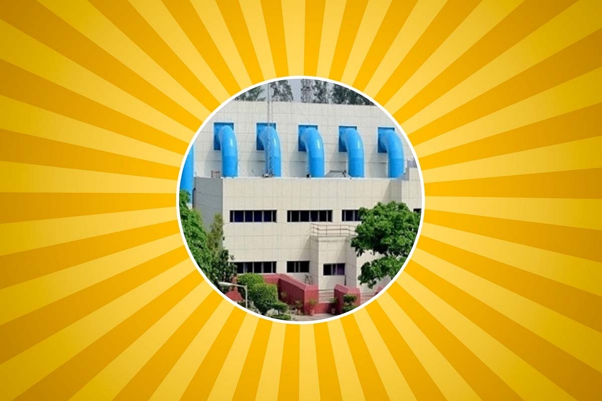
The Semi-Conductor Lab (SCL) in Mohali
This is the first of a three-part series titled “Rejuvenating India’s Semiconductor Ecosystem” (RISE) aimed at highlighting some of India’s existing capabilities in the semiconductors and discussing how to maximise them quickly.
India's new semiconductor scheme with an initial incentive package of nearly $10 billion was announced towards the end of 2021. By mid-February this year, the scheme received three proposals to build new commercial Silicon CMOS semiconductor fab (chip fabrication units); all three are awaiting 'yes/no' decisions from the Central government.
Going by the recent statements of Minister Ashwini Vaishnaw, the government is in "advanced stage of evaluation of the applications" and "we should have the first agreement signed this year".
Whichever applicant(s) get(s) approved, there is very little chance of their new fab in India reaching high volume production before 2026-27.
In the mean time, it will be worth while to take a closer look at India’s existing facilities and ecosystem with an aim of maximising their productivity and impact for the immediate future.
This series titled 'Rejuvenating India's Semiconductor Ecosystem (RISE)' is a thought starter and a call-to-action towards that.
The first part will look at Semi-Conductor Lab (SCL), which is India's first and currently the only semiconductor chip fab with full production lines of industry-grade equipment and infrastructure.
The second part will look at what can be achieved using 180nm Silicon CMOS technology that SCL has and the third part at the existing R&D fabs in academic and other similar institutions of India
SCL Mohali - a brief history
Quoting a bit from this report in EETimes, published in 2000, SCL originally stood for "Semiconductor Complex Limited" a Public Sector Undertaking (PSU) in India.
"SCL started production in 1983… A mysterious fire in 1989 knocked out the fab until 1997. The cause of the fire is still unknown, but there are suspicions of arson, since SCL was designing and developing VLSI technology for the military at the time" says the report.
More interesting is this line "SCL's revenues in 1999-2000 were about $14 million, with a profit of roughly $400,000." . If that is true, India had a profitable fab in 2000 despite the fire incident.
The next document that was referred to by this author summarises the 2005 situation - "..erstwhile SCL Company had accumulated losses of Rs. 132.39 crores as on 31.3.2005 which was more than 50% of its net worth, thus, making the Company a potentially sick unit. However, Government of India, taking into account the activities relating to microelectronics and the interests of the employees decided against disinvestment or sale of SCL Company. The Department of Space (DOS) restructured SCL Company into Society, namely, Semi-Conductor Laboratory Society (SCL Society) registered under the Society Registration Act, 1860 on 8.11.2005"
SCL remained "Semi-Conductor Laboratory" under ISRO from 2005-06 until 2022 when as per this press release, "SCL Mohali has also been handed over to MeitY from Department of Space and it is being opened up as a commercial fab for wider participation by Indian semiconductor design companies" .
Opening SCL as a commercial fab is a welcome move. Further, the government should also revisit the mode of registration of SCL as a 'society' and the "lab" that got added to the name together with it.
Some of the recent developments and opinions related to SCL (from December 2021 to present) are captured by Swarajya here , here , here and here.
Key technologies at SCL
Currently, as per the SCL website, there is a 6 inch (150mm) wafer size fab line for Micro Electro Mechanical Systems (MEMS) and an 8 inch (200mm) fab line with 180nm (0.18 micron) process node for CMOS - the latter seems to have been added around 2010-11.
A 2010 tender said, "Semi-Conductor Laboratory (SCL), SAS Nagar, is operating a 6” Wafer Fab. of 2000 wpm capacity in 1.2 micron /0.8 micron CMOS technology. SCL plans to upgrade its Wafer Fabrication Facility to 8” wafer fab at 0.18 micron technology node. The existing utilities like Ultra Pure Water (UPW) treatment plant and Effluent Treatment Plant (ETP) would require commensurate augmentation/expansion to support the 0.18 micron process"
It is interesting that the tender goes into minute details of the requirements for UPW and ETP systems. Anyone who reads through it will be left with no doubt that India is not new to the “ecosystem, infrastructure and know-how needed to operate fabs in India”.
Details regarding the addition of the 8 inch (200mm) wafer fab line with 0.18 micron (180nm) technology node are not fully publicly available.
However, at least two journal papers available in public domain hint that Tower semiconductors of Israel was the industry player that helped SCL in this regard. These publications also give a lot of insight into SCL’s capability and how chips can be designed and fabricated at SCL. These papers are:
1. SCL 180nm CMOS foundry: High reliability ASIC design for aerospace applications : H. S. Jatana and Nilesh M Desai, 2015, published by IEEE in 2015
2. From design to tape-out in SCL 180nm CMOS integrated circuit fabrication technology : Joydeep Basu (IIT Kharagpur), published by IETE Journal of education in 2019
This also points out to the possibility that a lot may be common between the 180nm technology of Tower semiconductors and SCL. A design done using the process design kit (PDK) offered by one should be manufacturable at the other as well - in other words, SCL most likely shares interoperability with Tower semiconductors for some or all of its 180nm offerings (The flavors that Tower Semiconductor offers within 0.18um can be found here , more on that later)
Capacity utilisation and optimisation at SCL
The SCL website had a Right To Information (RTI) page with information on a variety of matters - organisation structure, decision making process, budget and even a list of employees on payroll as of 31 March 2022.
However "Layout, Equipment Details and Photographs of Fabrication facility and other Infrastructure" were under the list of non-disclosure items. The RTI page currently shows "Page under construction" though some of the direct links still work.
The capacity of fabs are usually measured in Wafer Starts Per Month (WSPM) and there is no publicly available information on what is the possible WSPM for the 200mm wafer size 180nm process node fab line at SCL. Given that the chip orders had so far been limited to some of India’s academic, research and space application purposes only, the WSPM achieved over the past many years is likely to be much less than what the facility should be able to deliver in theory.
The exact number of equipment needed for a certain WSPM can vary from fab to fab based on the technology node and other factors; however, an approximate calculation is attempted here based on information available in public domain and some assumptions.
The scanners/steppers used for photolithography are usually the costliest. Photolithography is a must-need step for every "level" of processing, as that is where the design gets transferred (level by level) from the photomask to Silicon wafers (wafer by wafer, in hundreds or thousands).
'Level' here refers to say the active area, the gate, each of the implants, contact, each of the metals, via etc. A 180 nm node typically needs about 25 mask levels of designs to be transferred; the exact number will vary slightly depending on complexity of the chip .
See figure below where photolithography is at the centre, not all of the other key process steps may be there for every level.
The light source used in the scanner/stepper for photolithography varies depending on the resolution needed - in the case of a 180nm technology, levels that have the minimum feature size will need a stepper that has KrF laser (wavelength of 248 nm, which is Deep Ultra Violet) as its source whereas levels like the “fat metals” and large area implants can be done using an i-line (365 nm) stepper which is much less costly.
Information on the scanner/stepper used at SCL was not directly available on the SCL website, however in a “Record of clarifications provided to the queries of the prospective bidders during the Pre-bid Conference held at SCL on February 04, 2016..” ISRO clarifies that “SCL has NSR-S204B Nikon Scanner and NSR-2205i14E2 Stepper”.
NSR-S204B is a KrF based scanner as per Nikon’s website, however the throughput value is not mentioned there.
Websites like this and this have quoted a 120 wafers per hour (WPH) number as its standard throughput. NSR-2205i14E2 is an i-line stepper and its datasheet gives a throughput number of 103 WPH. While running in a production line, we also need to factor in "Overall equipment effectiveness" (OEE) as explained in this paper (summary diagram below).
As elaborated in the paper, the goal usually is to achieve an OEE of 60 per cent or more - assuming that and taking a 30-day month as average, the combined throughput can be 720hrs X (120 wph + 103 wph) X 60 per cent - that is 96,336 full wafer lithographic exposures. Dividing by 25 which is the average number of mask levels in a 180nm chip (design) we get a processing capability of 3,853 wafers per month.
To achieve that capacity for the 180nm production line of the fab, there has to be sufficient number of equipment for the other process steps (etch, implant, diffusion, deposition, growth, planarization, metrology etc) and automation with good overall efficiency.
As mentioned before, compared to the KrF scanner, these equipment are likely to cost much less. Also, out of the 25 mask levels, it is important to utilise the KrF scanner appropriately for the critical levels that need higher resolution and use the i-line stepper for the others. In other words optimising the loading of the tools is important
Interestingly, a 2019 “Invitation for Expression of Interest” which is still available on ISRO website said: “Semi-Conductor Laboratory (SCL) .. has an 8 ‘’ CMOS Wafer Fabrication facility comprising 67 processing, metrology, electrical testing, yield and other support equipment. SCL desires to automate the wafer-fab line and through this EOI, invites interested and competent parties to submit their proposal for the project”. Further developments on this are not known
Addressing some more factors often brought up as a challenge:
This section covers a few arguments that I have heard or read as challenges to a potential rejuvenation of SCL- in some cases suggestions are given as well.
a) Are the existing equipment too old and near the end of life ?
ASML, one of the leading wafer fab equipment makers has a section titled “extending product lifetime” on its website which says "A well-maintained ASML lithography system can last for decades – almost every system we've ever shipped is still in use at a customer fab”- this is true not just for the lithography equipment made by ASML but of other equipment manufacturers also and for most of the other key fab equipment as well.
In fact, as per a Nikkei Asia report in April, "Prices of secondhand chipmaking machines have soared over the past two years on ravenous demand". Fabs around the world will be keen on utilising their existing equipment to the maximum, including refurbishment if needed.
b) Is there still a market for 180nm ? Is it not an "outdated" technology ?
Here are some interesting reads - as per a recent article in ComputerWorld “the dearth in chip capacity is mainly for older semiconductors built on legacy logic chips, including, for example, 40nm, 90nm, 150nm, 180nm, and 250nm nodes” . The same is reflected in this slightly earlier article in SemiEngineering.
In another report this year it is said “200mm Shortages May Persist For Years”. To clarify, “200mm fabs manufacture devices at mature process technologies, ranging from the 6µm to the 110nm nodes” (so includes 180nm) and as per SEMI, the overall 200mm wafer fab capacity is about 6 million wafers a month
A more detailed look at product (chips) possibilities at 180nm technology, the revenues etc. will be dealt with in the second part of this series
c) Can SCL capture part of the market ? Does it have a good business process/plan ?
4,000 wafers a month, or over 2 lakh wafers in about 4-5 years is a very small number compared to global capacity. However each wafer will have many chips (how many will depend on the size of individual chip, examples in part-2 of this series) and this volume may be able to quench a good amount of India’s domestic needs in the category that can be made using 180nm technology. The aim should also be to try to get some exports - "Make in India, for the world"
At least three factors will be key in this effort:
First is to identify products that can be mass produced at SCL.
Second is to fine tune SCL’s business plan and operational efficiency to turn it profitable in a few years.
Third is to have an attractive business process to be able to match the expectation and satisfaction level of customers. For example, tedious tendering processes for every step (example making photomasks from design) may have to be replaced with predetermined vendors.
d) Does SCL really need 500-600 employees? Won’t the salary and pension for so many employees and ex-employees make it difficult for SCL to become profitable ?
A more accurate answer is possible only based on a detailed analysis of the current employee roles and skill sets, however here are some quick thoughts.
For the sake of argument, let us assume that there are “more employees than what may be an ideal number for reduced operational expenses” - given that SCL is now under MEITY it should be possible to reallocate those not interested to work in a fab to other offices.
New opportunities may also arise as part of the government's efforts to grow the semiconductor ecosystem in India, including in supply chain management, training etc.
Apart from opportunities in the government itself, it is quite likely that they will be able to find openings in the new private commercial fab(s) that are expected to come up in India in the next few years if they so desire - having worked for SCL as a commercial fab will place them at a unique advantage
In December 2021, Gautam Sarkar, seemingly an Indian defence enthusiast, came up with a compilation titled India’s Semiconductor Research Efforts : The Story So Far. This compilation gave multiple examples of chips fabricated at SCL already.
Commercial/Volume production potential for some of those will be examined in part-3 of this series, however the fact that they were successfully fabricated at SCL despite it not being fully automated, hints at a good percentage of the workforce being quite capable.
So. .
The brownfield semiconductor chip fabrication facility of SCL at Mohali is an asset which under capable leadership and with proper business plan can be run at much higher capacity commensurate with its operational capability. That will also enhance and reaffirm India’s readiness for the “next wave of commercial fabs”.
The government of India has already announced the goal to commercialise SCL. Now, Indian business houses should come forward to make it successful through joint venture(s), fabless companies (existing or upcoming) should come up with more products with market value that can be fabricated at SCL in high volume.
Introducing ElectionsHQ + 50 Ground Reports Project
The 2024 elections might seem easy to guess, but there are some important questions that shouldn't be missed.
Do freebies still sway voters? Do people prioritise infrastructure when voting? How will Punjab vote?
The answers to these questions provide great insights into where we, as a country, are headed in the years to come.
Swarajya is starting a project with an aim to do 50 solid ground stories and a smart commentary service on WhatsApp, a one-of-a-kind. We'd love your support during this election season.
Click below to contribute.
Latest