News Brief
SCL Commercialisation Under India Semiconductor Mission: MeitY Invites Proposal For Asset Valuation Of Fab Facilities
Swarajya Staff
Jan 27, 2022, 09:38 AM | Updated 10:19 AM IST
Save & read from anywhere!
Bookmark stories for easy access on any device or the Swarajya app.


The Union Ministry of Electronics & Information Technology (MeitY) has invited sealed quotations from registered valuers for undertaking the asset valuation of the ISRO-owned Semiconductor Lab (SCL) at Mohali.
As part of its recently unveiled $10 billion incentive package to build a semiconductor ecosystem in the country, the Government of India is pursuing options to commercialise SCL.
The government is likely to pursue its efforts to modernize and commercialize the brownfield semiconductor chip fabrication facility of SCL through a joint venture.
Formerly known as Semiconductor Complex Limited (a state-owned enterprise), it was moved under Department of Space in 2006 and renamed SCL.
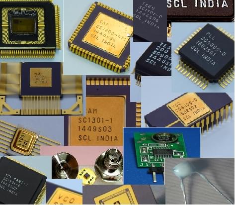
SCL has integrated facilities / supporting infrastructure all under one roof and undertakes activities focused on Design, Development, Fabrication, Assembly & Packaging, Testing and Quality Assurance of microdevices for various applications.
SCL currently has tools that can process starting wafers of 200mm size. In 2021, SCL sought to upgrade its fabs from a 180nm technology node to a 65nm technology node. It reportedly shared a proposal to MEITY for technology node upgradation
As part of its efforts to modernise SCL, the government is likely to ask MEITY to take over the SCI facility as part of "India Semiconductor Mission". SCL is currently operates under ISRO which is Department of Space.
SCL had a budget of nearly Rs.370 crore for operations and Rs 230 crore for Capex in 2019-20
The government is likely to look at several option for commercialising the operations of SCL.
While continuing with the existing 200mm production line, SCL may be asked enhance the capacity of the 180nm technology node. Even as recently as last week there are reports of chip shortage in 200mm production lines persisting for a few more years. This will however need swift action including a joint venture with a strong industry player to capture market
Adding (or converting into) compound semiconductor processing capability to SCL will be another roadmap that can be pursued. For Silicon CMOS fabrication, 300mm wafer size has been around for almost two decades, but many compound semiconductor fabs still predominantly process 150mm wafers.
There are reports that suggest "manufacturers are beginning to address this (challenges in existing production lines) by moving to the larger 200mm wafer sizes from current 150mm wafers: This could be an opportunity for SCL provided there is a strong technology partner willing to get into a joint venture or a technology transfer, as well as potentially an Indian business house who can ensure that effort is a commercial success
Another option could be to convert SCL into an "Intermediate Research Organization" (IRO) to bolster semiconductor manufacturing.
Also Read: Here Is Why Government Of India Is Trying For A JV To Modernise And Commercialise SCL Chip Fab In Chandigarh


