Tech
Talent Crunch For Semiconductor Engineers Worldwide — Can India Strike Win-Win Deals?
- The global talent crunch for semiconductor fabs can be an opportunity for India to "Train Indians for India and the World."
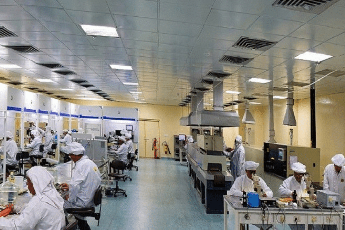
Employees at a semiconductor facility (Photo: Semi-Conductor Laboratory)
Earlier this month, there were reports (here and here) that contract chip manufacturing giant Taiwan Semiconductor Manufacturing Company (TSMC) "is having trouble getting engineers and keeping them on" in its foundries (semiconductor chip fabrication factories or fabs).
"TSMC said that its fresher employees that have been with the company for under 12 months had a turnover rate of 17.6%, missing the internal goal that TSMC had of 15% and is far, far worse than the average turnover rate of 6.8% within TSMC," one of the reports said.
Last week, the online news publication The Register published a story (likely a United States-centric one) in which it said: "While the global chip shortage shows some signs of subsiding, semiconductor companies are facing another area where demand outpaces supply: microelectronics engineers."
Chipmakers like Intel, TSMC, and Samsung are all trying to expand their manufacturing capacity in the United States (US), but this can't happen if there aren't enough engineers to design, fabricate, and verify the chips, among the other roles needed.
This is not the first time such concerns are surfacing — as early as January this year, EETimes reported that TSMC faces challenges managing employees at its new fab in Arizona who are unaccustomed to the long work hours and management culture, which in Taiwan have helped make the company the world’s largest chip foundry.
And in May, Nikkei Asia published a report titled 'TSMC faces uphill battle in U.S. talent war'.
Note that TSMC founder Morris Change has been warning the company against the proposed expansion in the US (See: Swarajya article from July 2021, Taiwan News article from October 2021, a podcast from April 2022).
Multiple factors may slow down the global expansion plans of chip-making giants like Intel, TSMC, and Samsung. The US is yet to approve the $52 billion package through the CHIPS Act and there are concerns expressed by industry leaders. Inflation and the anticipation of recession have led to some chip order cancellations. Semiconductor fab equipment delays continue.
However, given the cyclical nature of the semiconductor industry, and with the chip (IC) market expected to go from $500 billion (which it reached in 50 years) to near-$1 trillion by 2030-31 and, perhaps, $2 trillion by 2035-36, things are likely to pick up again sooner than later.
As for efforts to boost the semiconductor ecosystem in India, approval decisions are still awaited from the India Semiconductor Mission (ISM) on the three applications received by mid-February for applicants to build silicon fabs in India. After that, the incentive scheme is expected to be reopened for a second round of applicants.
The ISM seems to have taken baby steps towards building a talent pool in semiconductor design. Last week, while inaugurating the Digital India Week in Gujarat, Prime Minister Narendra Modi announced the first cohort of 30 institutions to be supported under the Chips to Startup (C2S) programme.
The C2S programme aims to train specialised personnel in the area of design of semiconductor chips at the Bachelors, Masters, and research levels, and act as a catalyst for the growth of startups involved in semiconductor design in the country. It offers to mentor at the organisational level and make available to institutions state-of-the-art facilities for design. This is part of the ISM to build a strong design ecosystem for semiconductors.
However, there is no clarity yet on how the ISM is planning to help build talent for new high-volume semiconductor fabs that are expected to come up in India in the next two to three years and start to be operational within another one to two years.
In fact, talent is needed not just after the fabs are in operation, but even to build the factory in the most optimal way, equip the production line efficiently for maximum capacity utilisation, and such that yield issues can be quickly addressed, among other reasons.
Perhaps, the global talent crunch for semiconductor fabs (building, operation, and analyses — at various levels of academic qualification) can be an opportunity for India to "Train Indians for India and the World."
India already has many engineers who take courses related to microelectronics and VLSI (very large scale integration) and, so, have a base in these domains. However, what they lack is exposure to the industry and the feel for how methods and mindset can be different in the industry as compared to academics.
Agreements can be worked out with Taiwan, the US, and other countries that plan to build fabs and, in return, the companies that would like to hire them should be asked to avail India's incentive programme (up to 50 per cent from the central government; states can offer more) when the scheme opens for a second round.
From among the Indian students who wish to get trained, those who are willing to stay back in India could avail the course at a lower fee than others who opt to work abroad.
Training can be provided in India by experts coming in from these industries under various sub-categories in a phased manner. For example, the ones related to building the factory and infrastructure can be the first to receive training, followed by those who will need knowledge about various equipment and to set up the automated production line.
In a few years' time, training can be more focused on operational aspects; for example, process development and matching, integration, yield, and so on. It is quite likely that a lot of NRIs (non-resident Indians) in the industry may want to come back to India to train people, test the waters, and, if they see a "fab future" for India, decide to stay back and work in upcoming fabs in India.
The research-and-development (R&D) fab facilities in various Indian institutes like the Indian Institute of Science (IISc) and the Indian Institutes of Technology (IITs) can be used and, as needed, selected trainees can be taken abroad for brief periods.
As a matter of fact, since industry fabs are mostly fully automated, chances of getting one's hands dirty directly on equipment are more in academic fabs than in the industry. Moreover, many industrial fabs now use virtual reality and augmented reality to be able to see and feel the operations from anywhere in the world.
As of now, this is just a thought starter. If the Government of India wants to think in this direction, it will need to quickly analyse all aspects and fine-tune the plan. Given that Prime Minister Modi has already declared that India wants to be a "chip maker and not just a chip taker," there is no doubt that India will need a good talent pool of engineers for building and operating fabs in the near future.
It is also a reality that many or at least some of the students who will get trained in India will have ambitions to work abroad; instead of lamenting the 'brain drain', why not use the situation in a way that can be a win-win for both the global semiconductor industry as well as for India?
Like "Make in India for the World" for semiconductor manufacturing (and, perhaps, more such strategic areas), we can consider "Train in India for the World."
(Inputs by Arun Mampazhy)
Support Swarajya's 50 Ground Reports Project & Sponsor A Story
Every general election Swarajya does a 50 ground reports project.
Aimed only at serious readers and those who appreciate the nuances of political undercurrents, the project provides a sense of India's electoral landscape. As you know, these reports are produced after considerable investment of travel, time and effort on the ground.
This time too we've kicked off the project in style and have covered over 30 constituencies already. If you're someone who appreciates such work and have enjoyed our coverage please consider sponsoring a ground report for just Rs 2999 to Rs 19,999 - it goes a long way in helping us produce more quality reportage.
You can also back this project by becoming a subscriber for as little as Rs 999 - so do click on this links and choose a plan that suits you and back us.
Click below to contribute.
Latest