Tech
Vedanta-Foxconn Asked For More Details On Semiconductor Chip Making Experience: What May Be The Way Forward?
- More details have been sought, reportedly, from the Vedanta-Foxconn joint venture on acquiring expertise for semiconductor manufacturing and fabrication or plans to rope in a third partner.
- What might be the road ahead for Vedanta in pursuing its semiconductor manufacturing ambitions?
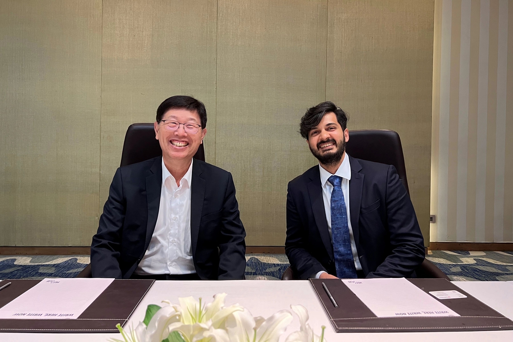
Foxconn Chairman Young Liu with Vedanta's Akarsh Hebbar (Global MD - Display & Semiconductor Business) (Photo: Vedanta Limited/Twitter)
The Union Ministry of Electronics and Information Technology (MeitY) has reportedly asked Vedanta-Foxconn joint venture to provide more details on how they plan to acquire the required expertise for semiconductor manufacturing and fabrication or their plans to rope in a third partner with demonstrated technical capability.
In December 2021, India unveiled an initial incentive package of nearly $10 billion to build a robust local display and semiconductor ecosystem. Under the silicon chip fab category, three applications were received.
Earlier this February, Swarajya published details of each applicant based on available information and calculations the day after the government announced their names. We calculated that the total investment planned by these three applicants are likely to be $13.6 billion, and the total incentives they may have sought is $5.6 billion.
Of the three, the international semiconductor consortium ISMC announced on 1 May that it will invest $3 billion to build a fab in India in partnership with Israel-based Tower Semiconductor (which is among the top 10 pure-play foundries of the world and is in the process of being acquired by Intel).
The consortium signed a memorandum of understanding (MoU) with Karnataka to set up a semiconductor manufacturing plant near Mysuru. It is reported to be seeking approval and grant of the incentives by August to move forward with project execution.
The second applicant, IGSS Ventures, signed an MoU with the Tamil Nadu government on 1 July for a proposed investment of nearly $3.2 billion, though there are a few concerns about the nature of their technology partnership.
Given that the total investment committed by the three applicants is likely to be around $13.6 billion, Vedanta-Foxconn's silicon fab investment plan could be about $7.4 billion. Vedanta-Foxconn has not yet decided on a location, though they have been talking to various states for at least five months.
According to a report in the Economic Times (ET), senior government officials have pointed out that Foxconn, the Taiwanese contract electronic manufacturing behemoth, has little demonstrated experience and capability in the large-scale fabrication of semiconductor chips.
"We are not very sure on how they (Vedanta-Foxconn) plan to achieve the scale that the government envisions. We want the companies to clarify on this," the ET report quoted the officials as saying.
Arun Mampazhy, in his article titled 'An Incomplete Story Of Foxconn's Attempts At Semiconductor Fabs', based on information in the public domain made an attempt to expand on Foxconn's attempts at semiconductor fabs.
There are two semiconductor fabs that Foxconn directly owns through acquisition — a 200 mm wafer size 130 nm technology fab, previously owned by Japan-based Sharp, and a 150 mm wafer size silicon carbide fab (which falls under the category of compound semiconductor fabs), previously owned by Macronix.
In addition, Foxconn has an indirect stake (through DNeX, a leading service provider in Malaysia's trade facilitation and energy sector) in SilTerra — a 200 mm wafer size fab with 180-110 nm technology owned by Khazanah Nasional Berhad, the investment holding arm of the Malaysia government.
However, none of these fabs fit into the type of technology that the Government of India has asked from applicants in the silicon CMOS incentive category — a 300 mm wafer size fab of 65 nm or below technology node.
Vedanta-Foxconn has applied for a 300 mm wafer size fab with technology node at 28 nm, and this is where government officials seem to have asked for clarification on where that technology is from.
Two days ago, Akarsh Hebbar, Vedanta Group's global managing director for display and semiconductor units, said Foxconn is currently running four foundries.
If we are to assume that three of these fabs that he is referring to can be counted as part of Foxconn's semiconductor portfolio, it is not clear which is the fourth one in question.
There are reports that Foxconn is planning a joint venture fab in Malaysia that will be processing 300 mm wafers using 28-40nm technology, but that cannot be counted as an operational fourth fab.
In December 2018, Foxconn claimed that it was building a fab unit in the Zhuhai area of China. However, no public information is available on what happened after that claim was made.
It is widely speculated that Bob Chen, a packaging expert who previously worked for Taiwan Semiconductor Manufacturing Company (TSMC) and is currently the head of Foxconn's semiconductor division, has a 60-member technology development team.
However, since the Government of India is asking for production-grade technology, it is doubtful whether this will qualify — almost the same concern that exists for technology from an R&D organisation like the Interuniversity Microelectronics Centre (IMEC).
If what is reported in today's ET is true, it represents a potential setback to Vedanta's ambitions to enter the semiconductor manufacturing space.
One way forward would be for Vedanta-Foxconn to get a third partner with demonstrated technical capability.
There are indications that the Minister of State for Electronics, Rajeev Chandrasekhar, may be travelling to the United States (US) soon. Part of his agenda, reportedly, is to meet semiconductor industry leaders, many of whom will also be attending the "Semicon West" conference next week.
Ajit Manocha, president and CEO of SEMI, is also one of the members of the 19-member advisory committee formed by India Semiconductor Mission.
Chandrasekhar (himself a chip designer with Intel and part of the Pentium team before he ventured into entrepreneurship and politics) is expected to woo companies like TSMC, Intel, Samsung, GlobalFoundries, UMC (all of which are pure-play foundries or offer foundry for contract manufacturing) or the likes of Micron, Kioxia, and Texas Instruments, which may fall under the category of integrated device manufacturers, to build fabs in India directly or in partnership with Indian companies.
It will also be interesting to see what will be the response from a company like Intel, which, if both its acquisition of Tower Semiconductor and the approval of the Tower Semiconductor-guided ISMC fab in India go through, could potentially look at "reviving" its 22 nm or 14 nm technology for foundry offering in India.
Whether Vedanta-Foxconn will opt for a third partner or be able to demonstrate that it has a running "65nm or below fab of high volume capacity" or a "production-grade technology" remains to be seen.
Another option for Vedanta will be to focus on its display fab proposal for which it has tied up with a strong technology provider, Innolux.
The total proposed investment by the two applicants in the display fab category is $6.7 billion, as per the government. Among the two, ELEST, owned by Rajesh Exports, has already confirmed that its investment is around $3.1 billion.
Vedanta's display fab application investment is likely to be $3.6 billion, out of which about $1.5 billion (Rs 12,000 crore is the cap on incentives for display fab) can be obtained from the central government. The various states in the race to lure chip companies will be willing to add a few hundred million dollars more as incentives.
The land requirements can also be "reduced" from the current 1,000 acres to 200 acres or so (with the possibility of expansion in future) — something that the states may be more comfortable considering.
Though Vedanta has repeatedly pitched the idea of an "integrated fab" for semiconductor and display, they are essentially two different things. Integration may be possible only at the product level; for example, display driver chips produced in the semiconductor fab and display panels produced in display fabs.
It may be prudent for Vedanta to take off on the display fab soon, assuming that the nodal agency is willing to fast-track approvals for the same.
Support Swarajya's 50 Ground Reports Project & Sponsor A Story
Every general election Swarajya does a 50 ground reports project.
Aimed only at serious readers and those who appreciate the nuances of political undercurrents, the project provides a sense of India's electoral landscape. As you know, these reports are produced after considerable investment of travel, time and effort on the ground.
This time too we've kicked off the project in style and have covered over 30 constituencies already. If you're someone who appreciates such work and have enjoyed our coverage please consider sponsoring a ground report for just Rs 2999 to Rs 19,999 - it goes a long way in helping us produce more quality reportage.
You can also back this project by becoming a subscriber for as little as Rs 999 - so do click on this links and choose a plan that suits you and back us.
Click below to contribute.
Latest