Technology
Chip Manufacturing Ambitions: Why India Should 'Learn To Sit Before Trying To Walk'
- If the government is serious about getting started in the chip fabrication business, it needs to start slow, build up the infrastructure, ecosystem and expertise needed, instead of trying to leapfrog into the major leagues by offering haphazard schemes.
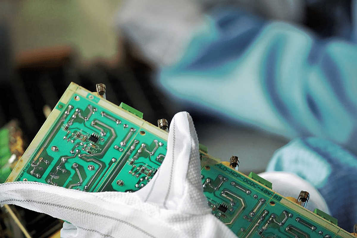
Semiconductors.
Newspaper headlines over the last few weeks have been abuzz with the news of an impending India-Taiwan semiconductor deal as early as the end of this year.
This deal is touted to be a gamechanger, if it does happen and that is quite a big 'if' given that our chip manufacturing ambitions have been much of a non-starter for the better part of half a century.
Our only tryst with semiconductor manufacturing, The Semiconductor Complex Limited, Chandigarh, was supposedly a state-of-the-art plant at the time but that dream literally went up in flames five years later in 1989.
This facility has been repurposed into some sort of a research and development facility under the Department of Space.
While flashy headlines are great for the incumbent government and its charismatic leader, whose efforts for self-reliance in all sectors of the economy have yielded what is at best mixed results, the reality is far from ideal.
The proposed facility, when it starts production in 2024 or so, will neither challenge Moore’s Law nor somehow propel the nation’s chip fabrication industry to the moon as proclaimed by self-confessed semiconductor experts and overzealous reporters with barely a faint idea of the complexity of setting up and operating a 28 nanometer, 300-millimeter wafer fab in a country where well-oiled logistics operations can come to a standstill for hours on end due to the domestic fauna wandering on to the nearest thoroughfare.
It has been quite entertaining for this old lithography engineer in a former life to read through the pages of wasted digital ink. Although, in defence of the clickbait loving press, they did mention that the Taiwanese had second thoughts about this plan due to the lack of infrastructure and an ecosystem.
The press corps exists to sensationalise every available bit of drab news, but what about the all-knowing bureaucracy in the Ministry of Electronics and Information Technology (MeitY)?
They are sure to have done their homework when they issued the notice inviting Expression of Interest (EoI) for setting up a semiconductor fab.
A quick review of the surprisingly brief EoI notice reveals that that may not be the case. They pretty much want the very investor they are trying to woo, to provide the MeitY with the proposed locations, roadmap for developing a raw material ecosystem and market feasibility.
The EoI would make one assume that we are doing a favour to the fab operators by inviting them to bring the most complex manufacturing technology known to mankind yet, just because we are willing to foot half the bill. It is high time we need to rethink our approach if we are really serious about getting into the semiconductor business.
Let us start by looking at the basic requirements for an ideal location for the proposed fab.
A clean environment, ie, low air particulate matter, abundant supply of clean, fresh water, uninterrupted and stable power supply, quick access to an international airport or seaport, first-world levels of road infrastructure from the said port to the fab and finally, close proximity to well-trained technical talent — the number of such locations could probably be counted on the fingers of one hand.
Even if one were to overlook these disadvantages, it will take a special customer to reconcile with the operational costs and problems they will bring.
Instead of the current approach, the government is more likely to attract a larger number of investors by employing a consultant to identify a viable location, acquire the land and develop a special economic zone (SEZ) which would encompass a complete semiconductor manufacturing ecosystem.
The monetary benefits being extended for setting up a fab should also be made available for all the ancillary units manufacturing specialty chemicals to cleanroom apparel.
Anything semiconductor grade is always held to a higher standard and they don’t come cheap. We need to build it before we even ask them to come.
The choice of technology is even more interesting. The EoI notice calls for 28 nanometer or lower node, 300mm CMOS device manufacturers and compound semiconductor fabs of 200mm or larger wafer size.
On paper, it makes sense to set up a 28nm or lower fab due to the fact that we sell more than 100 million smartphones annually in the country. Setting up a fab for a particular technology node is one thing, but running it and achieving yield is an entirely different game.
Scaling for Moore’s Law has been equally about quantum jumps in technology while maintaining continuous improvement. Technology transfer is achievable given time, money and will, but the tribal knowledge that goes with each node is not so easy to transfer, especially with an inexperienced domestic workforce along with communication and cultural roadblocks between them and the expat workforce.
Every OEM that has bleeding edge CMOS expertise has developed it through experiences gained from manufacturing older nodes and continuously building up on them.
That doesn’t mean we shouldn’t try it, but we need to understand that gestation periods for the fab to become viable will be much longer and the proposed timelines are going to be significantly off the mark.
Our arch rivals, the Chinese, have been at it for almost four decades now and they are still not a major player in this regime.
Compound semiconductor fabs and 200mm or 300mm silicon fabs that manufacture a wide range of integrated circuits with older technology nodes for industrial microcontrollers, power modules etcetera will be a good fit.
The requirements are less stringent and the fabs less expensive. These companies typically operate at much lower gross margins as opposed to the large fabs and OEMs.
A generous monetary incentive makes it viable for them to invest in a new fab, while getting us started in building the ecosystem we so badly need before we can think of building fabs for the latest technology nodes.
An automotive analogy is apt for the current scenario. We are trying to build a Formula One car having never built anything more than a go-kart. It is wise to follow the path of the automobile industry which has come a long way from assembling knocked down kits to designing and building modern cars.
If the government is serious about getting started in the chip fabrication business, it needs to start slow, build up the infrastructure, ecosystem and expertise needed instead of trying to leapfrog into the major leagues by offering haphazard schemes.
In other words, we need to learn to sit upright before we can walk.
Support Swarajya's 50 Ground Reports Project & Sponsor A Story
Every general election Swarajya does a 50 ground reports project.
Aimed only at serious readers and those who appreciate the nuances of political undercurrents, the project provides a sense of India's electoral landscape. As you know, these reports are produced after considerable investment of travel, time and effort on the ground.
This time too we've kicked off the project in style and have covered over 30 constituencies already. If you're someone who appreciates such work and have enjoyed our coverage please consider sponsoring a ground report for just Rs 2999 to Rs 19,999 - it goes a long way in helping us produce more quality reportage.
You can also back this project by becoming a subscriber for as little as Rs 999 - so do click on this links and choose a plan that suits you and back us.
Click below to contribute.
Latest