Technology
Interview With Industry Expert Dr Satya Gupta On India's Quest For Semiconductor Self-Sufficiency And Challenges Ahead
- Dr Satya Gupta, a former Intel executive and a successful serial entrepreneur in the semiconductor industry, has been very vocal about India's efforts at electronics self sufficiency and building semiconductor ecosystem.
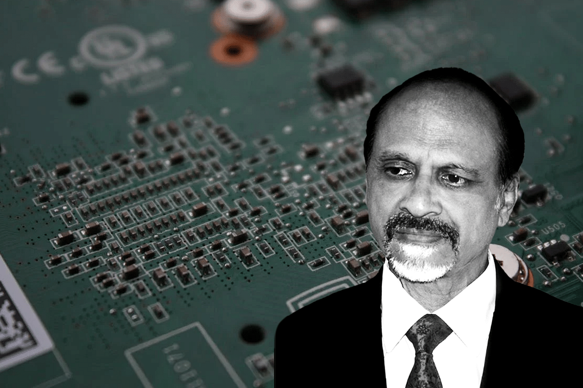
Dr Satya Gupta
Dr Gupta has been recently roped in as the CEO of EPIC (Electronic Products Innovation Consortium) Foundation, a non-profit organisation with the objective to create Indian electronics products and Indian brands in high-impact/high-volume categories and manufacturing semiconductor chips by scaling volume of Indian electronics products.
Swarajya contributor Arun Mampazhy caught up with him to understand his view on India's push to build a semiconductor ecosystem, the incentive scheme for chip industry, on design capabilities of India firms, addressing skilling challenges and host of other issues.
Here is an edited excerpts from the interview.
Arun Mampazhy: Please share with us your experience as a serial entrepreneur and how you compare it with working for a semiconductor behemoth like Intel?
Dr Satya Gupta: I always wanted to be an entrepreneur, and my mindset would always work like one.
My entrepreneurial journey started when I moved out of Intel and decided to form a turn-key ASIC and Foundry Service company, "Open-Silicon".
The biggest challenge was getting funding. As Silicon Valley was the right place to reach out to VCs, we moved from Portland, Oregon, to San Jose, California. We decided that we would give our best to raise funding for three months, and if we failed, we would go back and find jobs.
As our Open ASIC model was very sound and was well tested at IME, we were fortunate to land two offers, one from Sequoia (Pierre Lamond) plus Norwest (Promod Haque) and the second one from Goldman Sachs.
We decided to take up the offer from Sequoia plus Norwest as we felt their semiconductor experience and connections will be very useful. Thus the journey started.
After funding was accomplished, I came back to India and started building the engineering team and was very fortunate to find a young enthusiastic team wanting to do something unique and a leader Chitra Hariharan who moved from IME to join Open-Silicon.
We had a fun ride for the next six years, interacted with more than 400 global customers from the US, Europe, Japan, Israel, Europe, built relationships with all the leading Silicon Fabs and ATMP houses, all the EDA vendors and leading IP companies which were essential to the success of our Open Model.
We did more than 150 Tape-Outs for the global customers during six years using all the leading FABs like TSMC, Samsung, Chartered, UMC, Tower, Samsung, and SMIC. More than 20 of these projects went to high volume production, where Open-Silicon supplied the finished chips in large volumes to the customers.
In 2007 Open-Silicon was acquired by a Private Equity company at a $245 million valuation. Open-Silicon also won the "Best privately held semiconductor company by GSA in 2008". Open-Silicon and IME also produced a lot of leaders who are leading global MNC companies in India and globally.
Our entrepreneurial journey continued with the formation of Concept2Silicon System, which HCL acquired in 2015. We did multiple high-end ARM-based chips for leading global companies and also did the first HDR camera chip for the global leader in high-end mobile phones.
After two successful start-ups, we found the third one, SenZopt, an Electronics product company which built wireless and wire-free sensor technology for integrated Building automation, including lighting, air-conditioning, air quality and a fully automated parking system. Our parking automation solution implemented for one of the large semiconductor MNC won the best automated parking system award.
My 15 years of entrepreneurial journey was a roller coaster ride full of excitement and the ability to do quick innovations and build impactful teams.
I am extremely thankful for the experience gained at Intel which played a pivotal role in creating the right company structure, processes and systems and building the best and most impactful silicon engineering team.
Arun Mampazhy: From what time have you been also associated with organisations like IESA and VLSI Society of India. What kind of role do they play in boosting the semiconductor industry in India, and among the various organisations, is there a difference in focus?
Dr Satya Gupta: In 2005, some of the industry leaders got together and founded ISA with the charter to give a platform for the semiconductor companies in India, including MNCs, Design Services companies and Start-ups. I was fortunate to be part of the ISA founding team and served twice as IESA chairman in 2012-13 and 2020-21. During my chairmanship in 2012-13, we felt that Electronics is an integral part and key driver of the semiconductor ecosystem.
We transformed ISA (India Semiconductor Association) to IESA (India Electronics and Semiconductor Association). I feel that the major strength of IESA is the leadership which was composed of technology visionaries. Because of this, we were able to become a strong knowledge partner for the central and state governments and the electronics and semiconductor ecosystem. India's growth as a Chip design and leader and now on the path to semiconductor product and manufacturing leadership has vital contribution from the effort of IESA over the last 17 years.
VLSI Society was formed in the 1980's to focus on the other part of the ecosystem, that is, research, technology development, and strengthening academia-industry relationship. In 35 years of journey, the VLSI Design Conference and VDAT conference organised by VLSI Society of India has become the largest and most eminent international conferences bringing together global leaders from academia, industry and government to further research and technology development in the chip design and semiconductor areas.
As India will need increased trained VLSI Design engineers and semiconductor professionals, the VLSI Society of India has decided to form seven regional chapters to reach out to the maximum number of institutions and students.
Arun Mampazhy: In organisations or associations like these, different members may have various preferences depending on their professional background, the company they represent or own. Likewise, regional aspirations could also come into play - for example, if there is a project or scheme, members from a certain place may push to have it there.
When you are office bearer for such organisations, how do you take everyone along and keep the country's interest above all other factors?
Dr Satya Gupta: In both IESA and VLSI Society of India, we focussed more on growing the industry, the ecosystem and solving systemic industry issues rather than individual company issues. Some of the examples of this are the National Electronics Policy of 2011 and 2019, ESDM policies for various states, building start-up ecosystem with efforts like Electroprenuer park and SFAL, First Fab study of 2012-13, First in-depth report on India Microprocessor and many others.
For example, we worked on getting relaxation on environmental clearance for expensive used equipment, which helped everyone in the industry. Similarly, at VSI, we are working on building VLSI Design talent and building RISC-V ecosystem, which is the need of the hour for India, irrespective of individual companies' preference for a particular processor architecture.
Arun Mampazhy: How do you see the policy and $10.2 billion outlay announced by the government to boost the semiconductor ecosystem in India? In an interview, the minister said he sees six different efforts being supported - Silicon fabs, display fabs, compound semiconductor and similar fabs, OSAT/ATMP, design (fabless) and talent. Do you feel that there is enough emphasis and outlay for each of these subsegments?
Dr Satya Gupta: I have said on multiple forums that India's semiconductor policy and incentives provided under the policy are the best in the world and the most holistic.
Incentives of up to 50 per cent for the advance fabs and ATMP surely beats any other incentive policy across the world. Any industry for holistic development requires an emphasis on products, manufacturing, research, technology research and talent development.
The semiconductor policy of 2021 covers all these aspects in the most comprehensive manner, DLI for product development through start-ups and MSME, SMDP-C2S for research, technology development and growth of the technical and skilled workforce and the Indian Semiconductor Mission for developing the semiconductor manufacturing ecosystem.
I firmly believe India has a huge opportunity to become Power Electronics capital of the world by creating an end-to-end supply chain built around compound semiconductors like GAN and Silicon Carbide. This will help India's ambitions in the energy sector, electric vehicles and more efficient and smaller power supplies for every electronics product we use, from mobile/laptop chargers, desktop and servers, UPS, Inverters, air-conditioners all the way to Railway Engines.
For an overall balanced allocation of resources to cover all aspects of the semiconductor ecosystem, out of $10 billion, 85 per cent should be allocated to manufacturing ($8.5 billion), 10 per cent to product development ($ 1.0 billion) and 5 per cent for research, technology development and talent building ($500 Million). I had proposed a similar vision during the IESA vision summit 2020.
Arun Mampazhy: Among the various fab proposals that the government has already received, what is your assessment based on the information that has already come out in the public domain or based on what you may be aware of otherwise?
Dr Satya Gupta: As per public information available, five proposals were received. Three proposals for Semiconductor Fabs and two proposals for the Display Fabs. Most of these proposals have been under discussion for the last one year except the proposal from Vedanta and Foxconn for Silicon Fab and Rajesh Exports for the Display Fab.
I feel that most of the proposals are credible proposals. The major next steps for these consortiums will be to raise the required funding from institutional sources and find customers to load the fabs. Other than providing financial incentives to these proposals, the most critical job for ISM and the government is to do meaningful demand aggregation to utilise the wafer capacity to the fullest extent.
Arun Mampazhy: You have been part of the market study for various process nodes for potential fabs in India and presented some of those in forums and interviews. So far, the applications for setting up fabs in India seem to be all the foundry models. Do you see the possibility of an IDM- driven fab in India in future?
Dr Satya Gupta: All the current proposals for the fabs are for the foundry model. I believe India should pursue the IDM model in parallel, including Silicon and Memory fabs (DRAM and Nand Flash).
The foundry model requires to serve a wide variety of customers and products and will require large volume fabless companies to utilise the wafer capacity. The IDM fab will work on a limited number of their own products and will directly sell to end electronics products customers; thus, the business side of things are less complex.
Also, as the memory and processors get used in almost all the products and the market is growing rapidly, it will be good to create a strategy for getting a Silicon IDM or Memory fab to India. Intel, Samsung, SK-Hynix, Micron and Kioxia/Western digital can be potential for such an initiative.
Arun Mampazhy: Based on what the Government of India has set out as targets to achieve by 2026 as electronic production of $300 billion in India, a good estimate is that India will need $60 billion or more in semiconductors by 2026. Minister of State Rajeev Chandrashekhar recently said that the forecast is $70-80 billion worth of semiconductors by 2026. However, fabs will not be in full-fledged production by then, and even if they are in production by say, 2030, the amount of semiconductors consumed by India need not all translate into domestic demand.
In your opinion, what are the factors that the fabs coming up in India should focus on to ensure that they have sustained and maximum fab loading - for example, what should be the mix of domestic supply vs exports. Also, should the government introduce preferential market access for Indian fabs and/or import duties for those chips that we may be able to make in India by, say, 2030?
Dr Satya Gupta: To better understand the market size for semiconductors, we should differentiate between consumption and demand. While the consumption is growing fast, only about 10 per cent of current consumption can be considered semiconductor demand as the procurement decision for the other 90 per cent is not made domestically.
For the foundry business, the major customers are the large fabless companies like Qualcomm, Broadcom, NVidia, AMD, Apple, Microsoft etc., which are fab fillers.
We also have to factor in that the total semiconductor consumption is divided across various applications like IDMs, Memory, ASICs etc. and also across various technology nodes. I did a conceptual analysis of the foundry consumption across various technology nodes, and for example, 28nm foundry will be approximately about $1 billion, mostly coming from global fabless companies.
So, in general, a foundry has to plan for 20-30 per cent catering to domestic demand and 70-80 per cent for exports. Attracting large global fabless companies to fill the Indian fabs will also be crucial. The government has to play a significant role in providing fiscal and other incentives such as 10 per cent PLI type incentives to the fabless companies and, wherever appropriate, apply the preferential market access policy. Meaningful demand aggregation in the government and government-induced procurement can also play a significant role.
Arun Mampazhy: As for the domestic market for fabs, as they come up in India, how can we convert more consumption to demand?
Dr Satya Gupta: Today, only about 10 per cent of total semiconductor consumption can be considered a demand for the potential fabs. It will be fantastic if the demand can reach 25 per cent of the consumption by 2026, when it is expected to reach about 65 billion. The key to this is we have to grow Indian electronics product companies in all the high volume categories. Today Indian electronics products have less than 10 per cent market share of the overall consumption of electronics products of $180 billion.
Indian electronics product companies will generate the demand for semiconductors and have the power to decide which chip from which source must be used. If we can get a market share of 25 per cent or electronics products which are designed, manufactured and owned by Indian companies in the important segments like mobile phones, tablets, Wi-Fi routes, smart cameras, set-top Boxes etc., the demand for semiconductor products will also grow to 25 per cent of the consumption creating a significant domestic market for the fabless companies and fabs.
Towards this goal, we should select 10 high volume products and incentivise the Indian products companies to create Indian products through demand aggregation and policies like PMA.
To give an example, Indian demand for tablets in the education segment alone will surpass 100 million units in the next five years. Even if Indian tablets serve 25 per cent of this demand, it will create a market of $3.0 billion and semiconductor chip demand by the domestic companies to $1.0 billion. If the same can be done across 10 high volume categories, at least $10 billion of semiconductor demand can be added to the current projection.
Arun Mampazhy: What are your views on "Intermediate Research Organisations" (IRO) coming up in India in addition to commercial fabs?
Dr Satya Gupta: A Semiconductor technology research organisation along the lines of IMEC, CEA-LETI, IME-Singapore (NISER: National Institute of Electronics and Semiconductor Research), to focus exclusively on research and technology with a $500 million investment must be created. The research in future semiconductor technologies, sensors, mems, carbon nano-tubes, integration of various technologies at the packaging level at wafer-level, chiplets, interposers etc., will be crucial for long-term sustainable leadership in this strategic sector.
While creating such an institution, a strong focus should be on people and not just on research infrastructure. To achieve this is to involve global Indian technologists and researchers in a meaningful and institutionalised way.
Many global Indian technologists and researchers are very interested in contributing to this effort. Out of this initial fund of $500 million, $250 million should be spent on attracting the best of the minds to NISER, and $250 million could be invested in creating meaningful technology infrastructure. For an institutionalised and in-depth involvement of global researchers, a research grant of $10 million could be given to each, and they spend at least 50 per cent of their time at NISER.
With this model and full autonomy to do cutting edge research, India can create a very powerful technology development and research institute for long term sustainable leadership in this area. One of the other important factors is that the research IMEC should have significant involvement in the industry like IMEC has done.
Arun Mampazhy: Switching the focus a bit to design companies - as I understand, there could be predominantly two models - one where you do design as a service and two where you have your own products (ICs). Do we see more of the former kind in India, and if so, why?
We have seen a handful of Indian design companies getting acquired by MNCs from the US in the recent past. Why do you think we have not seen any of those design companies scales to the next stage to become Qualcomm or any other major product company? Is there a gap in terms of vision and aspiration of the founders or are there genuine limits for design start-ups in India?
Dr Satya Gupta: India is the world's design capital of semiconductor chips. All the semiconductor MNC's and most of the global start-ups have large captive design centres in India, designing the most complex chips for the global customers. These MNCs require additional design resources beyond their own employee pool, which creates good demand and business for the design services companies.
Secondly, design services companies need minimal investment, and the time to revenue is very fast, which is a proven model in the software services industry. The design service companies are consolidating through M&A and scaling pretty nicely.
On the other hand, the fabless semiconductor product companies require different mindsets and skillsets. Firstly, these companies require significant investment and a long gestation period. Typically, a medium complexity new chip with good commercial potential will take approximately $7-10 million investment and about five to seven years to meaningful revenues. Secondly, although India has excellent design talent, but we need better talent and focus on product conceptualisation, product marketing, business development and sales to create successful fabless product companies.
"A good CTO does not necessarily make a good CEO". DLI scheme by the government is a good positive initiative to address some of the issues related to funding and access to technology. Hopefully, we will see some good results in the next five years.
Arun Mampazhy: While talking about Designed Linked Incentives (DLI) as part of the recently announced scheme, Minister Ashwini Vaishnaw had listed four components needed for design companies - one is the tools used (for example, EDA tools), second is testing and verification, third is prototyping, and fourth is the IP.
Do you think that the DLI scheme offers enough support and roadmap for each of these aspects for Indian start-ups and small or medium companies to grow into product-based fabless companies, or do you see them helping more of design as a service kind of efforts?
Dr Satya Gupta: The DLI scheme is a progressive scheme to promote fabless semiconductor product companies in India. The four components listed by the Hon'ble Minister are vital, but the most important aspect of the DLI is the 50 per cent reimbursement of expenses incurred by the fabless companies. It is generally not understood, but the biggest cost for a semiconductor product company is people and operations related. Subsidising 50 per cent of any expenses, including people up to 15 crores, is a huge incentive. Facilitating access to EDA tools, fab, package, test, and IP is also very significant.
One other important vector is 4-5 per cent of PLI type incentives for chip deployment. In my humble opinion and based on experience in dealing with more than 400 global fabless companies and supplying millions of chips to customers, we need 15-20 per cent of PLI for semiconductor chips as the cost of wafers, packages, and the test is going to be much higher for Indian start-ups and MSMEs due to small volumes in the beginning. My dream is that Indian semiconductor companies should start consuming at least 1 million wafers per year in the next 10 years.
Arun Mampazhy: As I understand it, the DLI scheme itself has three parts to it - Design Infrastructure (DI), Product-Design Linked Incentive (P-DLI) and Deployment Linked Incentive (DLI). The government is hoping that about 100 design companies will use these schemes, and out of that, 10 or 20 may grow into the size of an annual Rs 1,500 crore turnaround company. Do you think that is a realistic goal?
Dr Satya Gupta: The goal of 100 fabless product design companies is completely realistic, and in my opinion, we should aim higher. China today has more than 1,000 fabless product companies and start-ups. Because of the incentives provided under the DLI scheme, I feel that companies with good products ideas will be better positioned to get funding from global venture capitalists (VCs), and I think over 25 per cent of them may be successful, which is an impressive success rate.
To achieve this success rate, we must carefully select the companies under DLI, that have meaningful product ideas and good chances of commercial success.
Coming to the point of 10-20 companies reaching Rs 1,500 crore ($200 million) will be tough in five tp seven years and will require a time horizon of at least 10-15 years. Even the most admired fabless company like Qualcomm took more than 10 years to reach these revenue levels. About 10 companies may reach a revenue of $20 million, five companies to $50 million, and two companies to $100 million or greater annual revenue in approximate 7-10 years horizon.
Arun Mampazhy: During the last few years, have we seen a slight uptick in the interest of Venture Capitalist (VC) and Private Equity (PE) firms in semiconductor start-ups in India.
If so, what, in your opinion, has been the driver of this change? Was there any shortcoming in the Indian risk capital allocation sector that avoided this domain for so long? Likewise, do you see big Indian business houses like Tata or Reliance or Adani group getting more and more into this field in the coming years?
Dr Satya Gupta: During the last 7-10 years, the global funding for semiconductor start-ups has significantly increased, which was pretty low earlier. AI/ML, IoT, 5G and EV, AV, and Industry 4.0 are some of the primary drivers of this momentum. Also, these applications need products and architectures which are much more diverse than traditional Von-Neuman architectures, thus more avenues for innovation.
Ten years back, who would have thought that companies like Cerebrus could build a chip which is full wafer. I strongly believe that good product ideas with a well-balanced team across technology and business aspects will find funding from domestic VCs or global VCs. Also, a few good successful exists by semiconductor product companies will set the role models and increase the risk appetite for the domestic VCs. Heartening to see Cosmic, Aura, Open-Silicon, and recently Saankhya are paving the path of successful exits in the semiconductor product start-up domains.
We are already witnessing signs of big business houses getting into the electronics and semiconductor domain for products or manufacturing, Jio Phone from Reliance, Tata Electronics Electronic Manufacturing and ATMP, Vedanta for display and Silicon fab. With the new semiconductor policy in place with $10 billion in incentives, I believe in the next couple of quarters, and we will see some significant announcements from the big business houses of India and globally.
Arun Mampazhy: How has the situation with respect to the availability of talented engineers changed in India during the course of your journey? What can the Indian government or university bodies do to address any remaining issues?
Dr Satya Gupta: During my semiconductor journey as the founder of Open-Silicon, I have been very fortunate to find very good young talent, eager to learn and make a significant impact on our companies and overall ecosystem later. Government programs like SMDP have been doing fantastic work for more than three decades in talent generation for the chip design.
The latest phase of SMDP-C2S is expected to train about 85,000 engineers in the next five years. With all the recent impetus in India and globally for chip design, this demand will probably shoot up to 200,000 engineers. We should think of revising the goals of SMDP and other talent generation upwards.
We should seriously consider and work upon a couple of ideas for sustainable talent generation. With the growing importance and talent requirement in VLSI Design and semiconductor manufacturing, it is of critical importance that we start an undergraduate program in Electronics and VLSI Design. It will tremendously help both in quality and quantity of the talent as bright young minds will be introduced to these exciting technologies early in their academic pursuit.
The Indian government has put a strong emphasis on RISC-V. Supporting these initiatives, we should start RISC-V based courses in our academic institutes and aim to produce 100+ RISC-V cores and SOCs from the academic research and development ecosystem in the next five years.
India's semiconductor manufacturing significantly in the next three to five years, and we will need a skilled workforce to run these facilities. We may need about 5,000 trained people in three years. We should leverage SCL Chandigarh to train people and start training programs with Singapore, Malaysian and Taiwanese semiconductor ecosystems to suitably meet domestic and global demand.
Arun Mampazhy: Can you take us briefly through your academic and initial career background, for example, being a Director for ASIC design at Intel?
Dr Satya Gupta: I graduated from BITS Pilani in 1983. After graduation, I joined IIT Delhi as a research scientist to work on a Silicon compiler to take a high-level description of a chip design all the way to Silicon.
We had done some impressive work with the guidance of Professor Anshul Kumar, but we were way ahead of time. After this I moved to Old Dominion University to pursue my PhD. During my PhD, I worked on parallel architectures and algorithms. I worked with NASA Langley for large scale CFD simulations on state-of-art parallel supercomputers like Thinking machine and CRAY. This steered me to join Intel post my PhD in their parallel supercomputing group, one of the most important and satisfying stints of my career.
At Intel, I was responsible for breaking the Tera-Flop barrier for the first time in 1993, bringing the laurels of fastest computer to the USA and also winning the prestigious "IEEE Gordon Bell Award for supercomputing". Post this I joined Strategic CAD Labs of Intel to work on advanced algorithms and EDA tools for microprocessor design and was part of the Pentium-Pro design team.
One day my colleague and Mentor at SCL, came to my cube and asked me to join hands with him to create Intel Micro Electronics (IME), a turn-key ASIC start-up within Intel. IME was a precursor to ICF (Intel Custom Foundry) and IFS (Intel Foundry Service). We soon realised that we must build a chip design team in India, and within a short span of two weeks, I moved back to India to start Intel India's first chip design team in 2000.
With a very small and efficient team, we did 26 chips at IME in just three years, from design to tape-out to packaging/testing and all the way to volume production for companies like Microsoft, Rockwell-Collins, Northup-Grumman as well as Intel's internal groups.
In 2003 with Intel's blessing, we took the IME's Open-Model external and founded "Open-Silicon" to start the exciting entrepreneurship journey. Alpha IP recently bought over Open-Silicon for $210 million.
Introducing ElectionsHQ + 50 Ground Reports Project
The 2024 elections might seem easy to guess, but there are some important questions that shouldn't be missed.
Do freebies still sway voters? Do people prioritise infrastructure when voting? How will Punjab vote?
The answers to these questions provide great insights into where we, as a country, are headed in the years to come.
Swarajya is starting a project with an aim to do 50 solid ground stories and a smart commentary service on WhatsApp, a one-of-a-kind. We'd love your support during this election season.
Click below to contribute.
Latest