Business
Exclusive Interview: Dr Harshad Mehta About Ruttonsha, Silicon Power And His plans For Silicon Carbide Semiconductor Fab In India
Arun Mampazhy
Mar 21, 2022, 06:05 AM | Updated 11:38 AM IST
Save & read from anywhere!
Bookmark stories for easy access on any device or the Swarajya app.
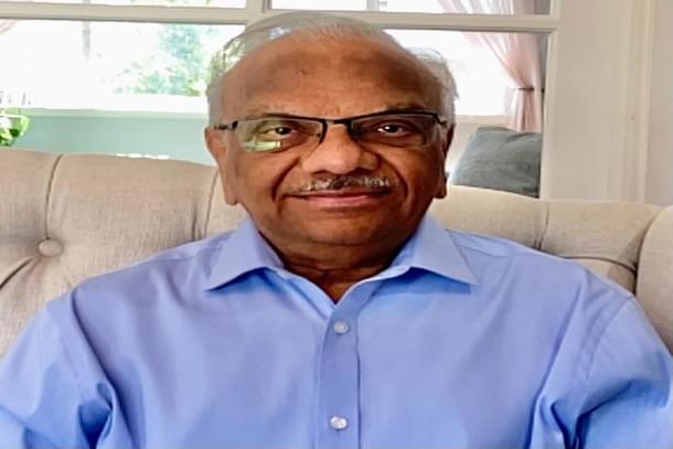

Here are key highlights from the interview
Thank you, Sri Harshad Mehta, for agreeing to answer some of our questions
1) Let me start with asking you about the history of Ruttonsha International Rectifier (RIR), Silicon Power Corporation (SPCO), Visicon Power Electronics Pvt Ltd (VPEPL), and how are they connected
International Rectifier (IR) as you know, was founded in the US in 1947 to make products predominantly for power management. Mr. Ruttonsha obtained a license from IR to make the products in India, hence the name Ruttonsha International Rectifier (RIR). Though it began in Mumbai, the facility was moved to Halol near Vadodara in Gujarat by around 1984. RIR was mainly focused on the low power segment within the power management devices.
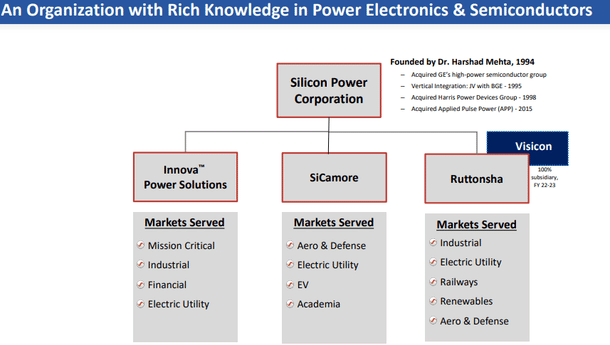
I founded Silicon Power Corporation (SPCO) in the US in 1994, and the earliest acquisition was the high-power semiconductor division of General Electric (GE). In 1995, we did a vertical integration through a joint venture with Baltimore Gas & Electric (BGE), subsequently acquiring Harris Power Devices group in 1998 and Applied Pulse Power (APP) group in 2015.
Meanwhile, after the passing away of Mr Ruttonsha, the founder of RIR, his successors had also started an Export Oriented Unit (EOU) in the late 1990s. Since Ruttonsha as a company focused on low power and SPCO focused on high power, we complemented each other. SPCO acquired Ruttonsha EOU in 2002 and later the parent company Ruttonsha in 2006. As a publicly listed company, since the name Ruttonsha is relatively popular in India, we have kept the name as it is
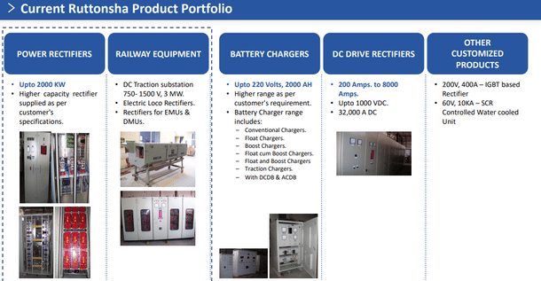
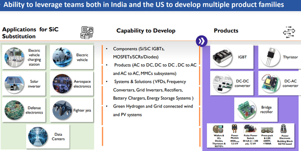
SPCO and Ruttonsha were focused on Silicon-based power devices until 2019; at that point, we felt Silicon had started reaching its technology limits, so we decided to get into compound semiconductors or, you may say, next-generation substrates. In the US, we acquired a Silicon Carbide (SiC) fab. We then started ViSiCon Power to focus on SiC-based products. Currently, Visicon is a 100% subsidiary of Ruttonsha. Overall, our current structure and current Ruttonsha product portfolio look like below.
2) Can you briefly touch upon the importance of Wide Band Gap semiconductor material (mostly compound semiconductor) in general and Silicon Carbide in particular for power applications and within power applications what is considered low or high power?
In the vast world of semiconductors, around 80% or more products are based on Silicon as a substrate that we see typically used for consumer electronics, communication, computation and power applications also to some extent. For less than 1000V applications, unipolar Silicon CMOS based devices are sufficient, but for handling voltages above that, we have to manage the forward voltage drop and heat dissipation within reasonable limits, so we need to have bipolar devices in which both electrons and holes conduct.
Insulated-gate Bipolar Transistor (IGBT) is essential for applications needing more than 1000 V. For applications involving more than 2000 V, Thyristors are used. Thyristors are composed of 4 layers stacked in PNPN type layer. With SiC, you can go to even higher voltages -- up to 10 kV with MOSFETs and up to 22 kV with IGBTs. This is a high-margin, niche segment in the semiconductor market. Our technology and experience in the power semiconductor segment is our key strength.
3) Please tell us more about the Silicon Carbide fab that you acquired in US - its capacity, what size wafers are being handled etc. Also, the market, competitors etc
Though there may be some overlap in the basics, it is quite a different world compared to the Silicon CMOS fabs, where with growing wafer size, you have economies of scale, and so in the latest fabs we see predominantly starting wafer size of 300mm. Those Silicon substrates do not need to be perfectly defect-free, whereas defect-free substrates are crucial in the case of power devices.
The SiC fab we have in the US handles 4 inch (100mm) and 6 inch (150mm) wafers. The devices made on them for high voltage applications are bigger in size - the IGBTs for example, could be 1 cm square, and the Thyristors could take up an entire 100mm wafer. In these cases, the substrate has to be completely defect-free, and so in general, the yield is inversely proportional to the wafer size - or in other words, it is difficult to scale to higher wafer sizes.
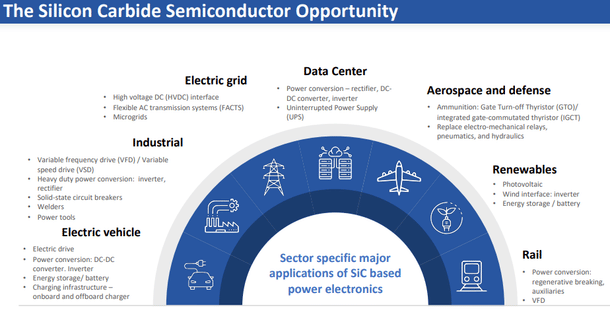
The SiC fab in the US is a 40,000 square feet facility with about 3000 wafers per month of 4 inch (100mm) equivalent. We are more focused on the high power segment (high power as opposed to the segment that deals with high volume commercial applications like electric vehicles). We cater to Electric Utility companies, Industrial Customers and certain defence and other strategic segments. Our competitors are companies like ABB, Siemens, Mitsubishi, etc.
4) What are the SiC plans for India? What are their investment targets and timelines ?
Our India plan for SiC-based products is in three phases.
Phase 1: Making the SiC wafer. Since the full thickness of the wafer does not need to be completely pure, we start with a regular SiC wafer and, through epitaxial processes, deposit pure SiC to the required thickness on top of that. This itself gives us sellable products because many companies want to buy this "ready to make devices" SiC wafers. Our Phase1 plant in Halol is 90% complete already and is expected to be fully functional by around June 2022.
Phase 2: This is building the fab that can do the device fabrication, and the output will be the processed wafers.
Phase 3: Dicing the devices from the processed wafers and packaging them.
This is the order in which the process flow happens. However, after Phase 1, we are focusing on Phase 3 and hoping to have that facility ready sometime between Dec 2022 and Mar 2023. Since we already have a running fab in the US, getting the Phase 3 facility up and running in India will help do some of the packaging here.
The three phases together need an investment of about 175 to 200 crore INR, out of which Phase 2 is the more investment heavy phase requiring about 150 crore and we are hoping that it will be up and running by the second half of 2024. The fab we are hoping to build in India is mostly similar to the one already in the US, including the capacity aimed for. Out of the total 175-200 crore needed, we have raised about 40-45% through loans, we are also looking for investors and equity partners for the remaining.
5) What is the status of the proposals you have submitted to the government of India for various incentive schemes?
One year ago, we applied the SPECS scheme. We have also submitted an application under the latest $10 billion scheme for semiconductors, which the government of India acknowledged on the 19th of February this year.
Though there is a recognition at the top policy-making level in India and the Minister for Electronics himself has said that compound semiconductors is a relatively low hanging fruit for India and can be quickly promoted and made one of India's strengths, bureaucracy is bureaucracy. Some of the requirements seem very illogical. For example, for every piece of equipment that is planned to be bought, we are asked to submit at least three quotes. Now, some of these are equipment we will be buying only in 2024 and it is very unlikely that equipment providers give quotes this early. Likewise, in spite of Visicon being wholly a subsidiary of Ruttonsha now, a 10-year lease agreement between the two was asked for. I hope that the government can see that some of these unnecessary complications can be avoided, and the process can be made faster.
6) In spite of a relatively lower investment requirement, by mid-February of 2020 Visicon Power's proposal was the only one received by the government of India in the compound semiconductor bucket. Indeed, there is time till 1 Jan 2025 to apply, but if we don't see a big rush to apply, what do you think could be the reasons?
Know-how of the technology and market is extremely important in this segment. It is also a field that requires multidisciplinary domain knowledge. In addition to the electronics side of semiconductors, the material side is an important aspect. Likewise, understanding the power devices and the market segment and many more such factors. You can't just get into this segment one fine day.
7) Are you hoping to get into more areas within the compound semiconductor segment, for example, Gallium Nitride (GaN) based products ? Or Silicon CMOS
As I said before, our strength is technology. We are not a big company with the ability to invest huge capital in cutting-edge Silicon CMOS fab and wait for 10-12 years for it to be fully profitable, and so we are not currently looking at that. As for GaN, we did submit an Expression of Interest(EoI) to the government, but with the kind of processes it takes, especially with the bureaucracy, we are rethinking if we should submit a full-fledged proposal or for now, tag along with the IISC-MEITY Gallium Nitride (GaN) Ecosystem Enabling Centre and Incubator (GEECI) for which government has approved Rs 298.66 crore.
8) What are your expectations about R&D in India, especially for the kind of fabs and facilities you hope to start?
Our facilities are centers of excellence in what we do, and in addition, we have tie-ups with IIT Delhi for the material aspect, IIT Chennai for the device aspect and IIT Bombay for the application aspect. Likewise, we have collaboration with many other academic and research institutes in India and that should help build the ecosystem.
9) What about the skilled manpower that may be needed for these upcoming facilities in India
As I mentioned, through the academic collaborations that we have, there are students already doing internships at our facilities. In the future, we are also confident that we will be able to find or train the required manpower and skill set in India.
Thank you once again Sri Harshad Mehta, and wish you good luck and success in all your plans
Arun Mampazhy has a BTech from IITM and MS from University of Maryland in semiconductor fabrication and over a decade of industry experience. His dreams of seeing a commercial fab takeoff in India has changed from black and white to colour over two decades. He can be reached via email nanoarun(at)gmail(dot)com or @nano_arun on twitter. Views expressed are personal.


