Technology
Leadership, Institutionalisation, Speed And Training - A WishLIST For 'India Semiconductor Mission'
- The criticality of India's push for manufacturing semiconductors cannot be overstated.
- Here are a few ideas for ensuring the project gets off to a solid start.
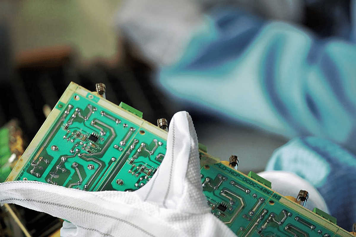
Semiconductors.
On 30 December 2021, in an event that received scant media attention, Union Minister for Electronics and IT (MeitY) Ashwini Vaishnaw launched the portal for "India Semiconductor Mission" (ISM). The portal currently serves as a "single window for registration and filing application for schemes on Semiconductor & Display Fabs".
The applications for setting up fabs under the $10 billion incentive package of the government opened on 1 January 2022, and the portal launch was timely. Currently, the portal displays notifications, detailed guidelines and application process for Silicon CMOS, display and other fabs as well as OSAT. The website for Design Linked Incentives (DLI) schemes was launched on 12 January 2022.
For now, ISM's top priority is to get as many globally reputed companies to apply for fab and OSAT units- either directly or through its Indian business partners, as possible.
Minister of State for Electronics and IT, Rajeev Chandrashekhar, has already hinted at the government proactively reaching out to the likes of TSMC, Samsung, Intel and so on.
For now, the deadline for applications for display and Silicon CMOS fabs are "45 days from 1 January 2022", however, the portal also says it is extendable. While ISM is likely to try all it can to make global players apply before mid-February (and then negotiate as mentioned in the policy), it is also keeping the option for a deadline extension open, in case it is needed.
While we have two accomplished technocrat-entrepreneurs at the helm of affairs as Ministers at MeitY and both have demonstrated ability to drive initiatives from day one of their tenure, one cannot expect them to micromanage ISM, including being at the negotiating tabl with every interested party or applicant.
ISM will be the nodal agency, which in most cases will review the applications and forward its recommendations for final approval. Needless to say, professionalism from top to bottom will be a must, so also a corporate culture that not only matches global standards but can also address the unique Indian context.
To put it in a different way, ISM should be an enabler, while also being an agency that ensures quality, compliance and standards - and what better way to do this by setting an example in itself and being a role model.
The ISM as an institute will have a critical role role to play in coordinating between other ministries (Defense, Commerce, for example), academic institutes and research organisations, industry associations, media etc.
In a June 2020 article in ORF as well as in articles in Swarajya, I had shared a few thoughts involving various levels of coordination - MOSIS like arrangement for academic or startup chip orders, Trusted Foundry model for defence etc., to name some.
The National Policy on Electronics, 2019 (pdf) too has a lot of ideas - see in particular the sections on "Industry-led R&D and Innovation", "Trusted Electronics Value Chain" and "Cyber Security". In fact, the idea of 'trusted foundries' is already mentioned in 5.18 which reads:
In other words, ISM most likely does not need to spend much time to study what all it should be doing. The NPE-2019 seems quite comprehensive, the amendments and tweaks can be made along the way based on feedback from the players using the scheme. The focus should be in realising those goals in a timely fashion.
The "HML" undergoes periodic updates, for example, this from 24 August 2020. So that one goal in the NPE-2019 can be fulfilled by adding semiconductor and display fabs too to this list. For an industry that is Capex intensive and has a high gestation period, such a move will help credit availability through funding agencies over and above what the government of India is offering as fiscal support which is a maximum of 30 per cent to 50 per cent of project cost or Capex, based on kind of fab.
As India is relatively late to the game, speed of execution and enablement will matter a lot for ISM. While indications are that the government of India would like to have some "big names" set up shop in India, it is also important to make sure that the 'relatively' smaller ones are not ignored or de-prioritised.
Nothing succeeds like success, and ensuring that one or a few relatively smaller fabs take off soon is likely to help trigger more interest from the bigger players. Speed of execution, apart from empowerment of ISM to take quick and firm decisions, also will need human resources in adequate quality and quantity.
That leads us to the final topic from the wish LIST, the training needed for the potential employees of the fabs and OSAT units that will come up in the next one or three or five years. There is a "Human Resource Development" section in NPE 2019 that covers a range of topics, but does not specifically talk about skilling for fabs.
Government of India had been running the "Special Manpower Development Program" (SMDP) and SMDP-C2SD (C2SD being Chips to System Design) since December 2014. And now a newly launched "Chips to Startups" (C2S - website) program summarises the existing programs and gives out a new call for proposals.
As in any big effort of this nature, certain challenges will come along. For example, the possibility of private training programs and institutes sprouting with promises of job offers, which in itself is not a bad thing as long as the quality standards are met - regulations or certifications for such efforts is something that ISM can think off.
The SASTRA University in collaboration with Tata Electronics Pvt Ltd (TEPL) and Taiwanese Universities, launched an MTech course last year with "one year of the course at SASTRA University's campus in Thanjavur and the second year in either Asia University or Yuan Ze University in Taiwan. Second-year curriculum would consist of practical experience in major lab facilities, a six-month industry internship in Taiwan’s advanced semiconductor manufacturing industry and basic Chinese language skills".
In the global scenario of need for increased workforce in the semiconductor industry, one wonders how such trainees can be made sure to stay back in India as opposed to being absorbed into the country where they do industrial training or other countries of opportunities.
For example, as per a report, the US alone will need to add 70,000 to 90,000 silicon workers by 2025, so quite likely any training programs offered for Indians will also be viewed by at least some as an opportunity to go abroad.
ISM can perhaps view this as an opportunity rather than as a challenge - maybe work out a mechanism to make the training a 'profitable' venture too from among those who would like to go abroad and use that to incentivise those who are willing to stay back and help India in one of its most crucial journeys of this decade.
Introducing ElectionsHQ + 50 Ground Reports Project
The 2024 elections might seem easy to guess, but there are some important questions that shouldn't be missed.
Do freebies still sway voters? Do people prioritise infrastructure when voting? How will Punjab vote?
The answers to these questions provide great insights into where we, as a country, are headed in the years to come.
Swarajya is starting a project with an aim to do 50 solid ground stories and a smart commentary service on WhatsApp, a one-of-a-kind. We'd love your support during this election season.
Click below to contribute.
Latest