Tech
A Semiconductor Material Better Than Silicon? A Quick Look Back To Not Get Ahead Of Ourselves
Arun Mampazhy and Karan Kamble
Sep 07, 2022, 04:12 PM | Updated 04:23 PM IST
Save & read from anywhere!
Bookmark stories for easy access on any device or the Swarajya app.


Do we now have the best semiconductor material ever to exist?
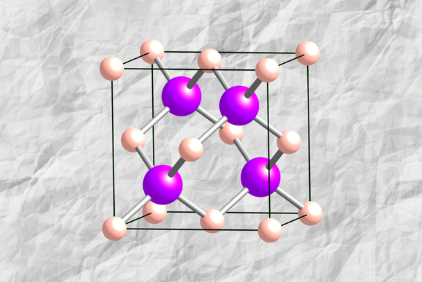
Researchers at the Massachusetts Institute of Technology (MIT), the University of Houston, and other institutions have found that a material known as cubic boron arsenide performs better than silicon.
Silicon is considered to be a foundation of a lot of modern technology, but this new material is faring better than silicon in a couple of aspects that may matter for some kinds of chips.
High thermal conductivity and electron-hole mobility are crucial for electronic and photonic devices. Though silicon is widely used, it is said to be less amenable to “holes” — the positively charged counterparts of electrons — than it is to electrons and it isn’t even the best conductor of heat going around.
Cubic boron arsenide apparently overcomes both of these limitations of silicon. Its thermal conductivity especially has been found to be almost 10 times greater than that of silicon. This, along its with much higher mobility in comparison to silicon, is said to make it a promising candidate for next-generation electronics, according to an MIT news report.
The findings were published in the journal Science in June this year.
For all its promise, though, the MIT news report has said about the material: “More work will be needed to determine whether cubic boron arsenide can be made in a practical, economical form, much less replace the ubiquitous silicon.”
This next step, of finding practical and economic ways to make cubic boron arsenide, is where the challenge is at, and has been with other candidates in the past.
Silicon As A Semiconductor
This is not the first time that there is talk of replacing silicon with a better semiconductor material. It may be worthwhile to take a brief look back in time, though this won’t be a comprehensive account by a long shot.
There’s an excellent paper on the history of semiconductors published 2010 in the Journal of Telecommunications and Information Technology.
In there, one will notice that in the first three sections, the word “silicon” doesn’t even find a mention. Much of the “theory” of semiconductors, including the Hall effect used to measure semiconductor properties, were proposed independent of silicon.
In fact, even the first patented device using semiconductors — point-contact rectifiers (early form of diodes), patented by Sir Jagadish Chandra Bose in March 1904 — were not silicon-based. Bose’s focus was instead on galena, or lead(II) sulphide (PbS).
Slightly over two and a half years later, a patent obtained by G W Pickard, titled ‘Means for receiving intelligence communicated by electric waves,’ mentions silicon. This is, perhaps, one of the earliest uses of silicon as a semiconductor.
Around the same time as silicon, silicon carbide crystal detectors, too, were patented. In fact, different types of crystals were in play while making, say, crystal detectors (“cat’s whisker”) for vintage radios. According to this crystal detector explainer, silicon, although popular initially, was rarely used during the 1920s.
Much of the credit for bringing back silicon, so to say, belongs to Russell Ohl, the inventor of the p-n junction.
A paper, titled ‘The origins of the pn junction’, published June 1997 in the periodical IEEE Spectrum, called Ohl “an unsung hero of semiconductor history.”
After all, Ohl’s investigations with silicon over the second half of the 1930s paved the way for technology that powers today’s solar cells.
Ohl's p-n junction itself became an all too common choice for the electronics industry and a basic building block in the design of semiconductor devices.
Silicon’s Rise
The first transistor, successfully demonstrated in December 1947 at Bell Laboratories by William Shockley, John Bardeen, and Walter Brattain, did not use silicon. The semiconductor used was germanium.
However, it was known at the time that “silicon would be a better transistor material than germanium for most applications.” This is because of the higher energy gap of silicon, which was 1.1 eV, compared to 0.67 eV for germanium.
However, factors like higher energy gap, among others like the significantly higher melting point and chemical reactivity of silicon, also brought along disadvantages.
Still, with the scales tipping in favour of silicon, the material was continually tweaked until, in 1954, the first manufacturable silicon transistor was made. Further development led to silicon taking precedence over germanium on the whole.
“As technology developed, the relative ease of fabrication of silicon devices made them ever more dominant, while germanium tended to occupy special niches—a situation that still prevails,” Ian M Ross writes in the paper ‘The Invention of the Transistor’, published January 1998 in the Proceedings of the IEEE. (Recommended reading for those interested.)
Interestingly, an “element of luck” was also said to have been involved in silicon turning favourable to the electronics applications sought by scientists and engineers.
“We surely were incredibly lucky to find one material and its oxide with which we could fabricate and encapsulate high-performance transistors and IC’s,” Ross writes.
All this is to say that silicon was not an obvious or natural choice. In some sense, it fought its way through and secured its place.
Now, sitting in gazillions of chips (integrated circuits) and other semiconductor devices, silicon must be reading claims of the discovery of a material “superior” to itself, one that is even tagged as the “best semiconductor material ever.”
With a smile, it must be saying, “Sure, bring it along, I have room for you all.”
What's meant is this — even today, silicon is not the “one and only” material used as a semiconductor (some alternatives mentioned here).
While there are semiconductor devices made from a different “starting material,” there are also some examples of different materials being “inserted” into the base silicon to achieve various properties.
For example, the Taiwan Semiconductor Manufacturing Company claims to use silicon-germanium (SiGe) as the channel material for certain devices (p-type FinFET). There are also known examples of strained SiGe for mobility enhancement and similar use of silicon-carbon.
Silicon Alternative?
Whether with these examples or in the case of cubic boron arsenide, a key improvement sought is mobility — mostly of “holes,” which are the positive charge carriers (as opposed to electrons).
It is sometimes asked: “Aren’t holes just the absence of electrons? So, why are their mobilities different?”
The easiest escape answer to that question is that mobility in semiconductors cannot be understood in the “conventional” sense. (A discussion for those interested.)
What's relevant for us here is that one of the key claims in the case of cubic boron arsenide is the “ambipolar mobility.”
In addition to the paper by Shin et al, another paper by a different set of authors was published in Science on the same day, 21 July 2022. It appears that as part of a collaboration, the Chinese group helped in coming up with the measurement setup.
What’s interesting is that the discussion that follows the need for a special measurement setup boils down, yet again, to the ‘purity of the sample’.
It is possible that cubic boron arsenide could be seen as “yet another” mobility enhancement possibility.
The other key property that has made this material a candidate of interest is the high thermal conductivity. As more and more transistors began to be packed in the same area, heat dissipation emerged as a big challenge. (A quick read on how the industry deals with some of these challenges.)
But there are many other properties, such as long-term stability, that are important and yet to be tested.
Above all, cubic boron arsenide may still be far from being considered for making in bulk. Thus far, the material is said to have only been made and tested in small, lab-scale batches that are not uniform.
It bears repeating, therefore, as the MIT news report itself puts it, the challenge "is to figure out practical ways of making this material in usable quantities." Replacing the ubiquitous silicon is still a faraway goal.
Till such breakthroughs happen, cubic boron arsenide can, perhaps, be added to an existing list of candidates — though not exactly all of them for the same reasons — made up by the likes of transition metal dichalcogenides (TMD) and carbon nanotubes (CNT).
Until any of them provides necessary confidence as a real commercial possibility, silicon will remain the key semicon.
Arun Mampazhy has a BTech from IITM and MS from the University of Maryland in semiconductor fabrication and over a decade of industry experience. Karan Kamble writes on science and technology for Swarajya.


