Technology
The Compute Bottleneck In The Path To India's AI Sovereignty... And Why We Must Build Our Own Semiconductor Industry
Arpan Sow
Sep 15, 2025, 03:16 PM | Updated Sep 16, 2025, 11:43 AM IST
Save & read from anywhere!
Bookmark stories for easy access on any device or the Swarajya app.


"Prometheus stole fire from the gods and gave it to man. For this defiance, he was chained to a rock, his liver devoured daily by an eagle. Fire, once a divine monopoly, became the spark of civilization."
Today, we stand at a new Promethean threshold. Artificial Intelligence (AI) is the fire of our time — a force as transformative and dangerous as the flame once stolen from Olympus.
From scientific discovery to national security, from climate modelling to space missions, AI is becoming the infrastructure of thought, the scaffolding of the future. The world's most powerful nations have recognised this reality. The United States (US), China, and the European Union (EU) are not merely investing in AI; they are weaponising it, embedding it, and owning it.
At the core of this global contest lies the most strategic layer of the AI stack: the foundational model. These large-scale, general-purpose models — trained on vast oceans of text, images, code, and signals — power increasingly commonplace applications like chatbots, autonomous agents, medical diagnostics, and legal analysis.
But these models aren't neutral. They actively prioritise what to say, what to suppress, what to predict, and how to act. They shape global discourse and decision-making. The giants — OpenAI, Google, Meta, Baidu, Huawei — are locked in a fierce race because they understand a fundamental truth: whoever builds the model writes the future.
What does this mean for a nation that lacks sovereign foundational models? It means speaking through systems that were not trained to understand your languages, your values, your reality. For India, such an outcome represents not just digital dependency but a civilisational risk.
The Gap: India's Precarious Position
Despite being home to 140 crore people, a thriving information technology sector, globally admired STEM (science, technology, engineering, and mathematics) talent, and a deep civilisational legacy of inquiry and knowledge, India remains largely on the periphery of this foundational AI race.
We talk of sovereign AI but lack the foundation — access to large-scale compute, open and diverse datasets, research depth, institutional collaboration, and a clear national mission to build and govern our own foundational models. We are building applications on top of others' architectures because insufficient infrastructure prevents us from conducting meaningful work at fundamental levels.
This reality forces a sobering question: if India does not rise to this moment, will it merely fall behind — or will it be encoded out of the future entirely?
The Foundations Required
India must build sovereign foundational models grounded in its languages, values, diversity, and strategic interests. The success of any foundational model hinges on four key pillars: compute, data, talent, and application perspective.
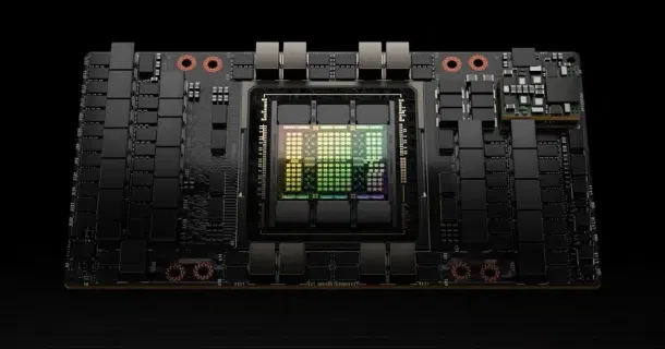
Of these four, compute stands as the most critical bottleneck. 'Compute' refers to the immense processing power — thousands of high-performance GPUs (graphics processing units) and AI accelerators — needed to train models at scale. Without compute, data and talent remain inert resources.
India's current access to compute is minimal, fragmented, and heavily reliant on foreign providers, with limited sovereign control. We face export restrictions on cutting-edge chips and lack indigenous hardware capabilities to build and supply compute infrastructure comparable to global leaders.
Understanding the Scale: The Numbers Behind Modern AI
To appreciate the magnitude of this challenge, consider the computational requirements for training cutting-edge models:
Training a 600-billion-parameter multimodal model requires an estimated 20,000–30,000 NVIDIA H100 GPUs operating for approximately 60 days. This accounts for the model's 2.4 terabytes of weights, 7.2 terabytes for optimiser states, and the computational demand of 36 sextillion FLOPS.
For perspective, xAI's Grok 3 — a multimodal AI model with an estimated 600-800 billion parameters — was trained using roughly 100,000 NVIDIA H100 GPUs in the Colossus supercluster, consuming about 200 million GPU-hours to achieve state-of-the-art performance in reasoning, mathematics, and coding.

The India AI Mission's selection of multiple firms to build indigenous foundational models reflects global recognition that speed often trumps efficiency in the AI race. To ensure minimum training turnaround times and maintain competitiveness, these firms require colossal-scale compute capacity.
As AI evolves toward agentic and physical robotic embodiments — humanoid robots and autonomous vehicles becoming part of everyday life — the computational demands will only intensify. The new ocean of data from deployed AI systems will require even greater compute capabilities to ensure models remain safe and effective in real-world conditions.
OpenAI's 'Stargate' initiative exemplifies this trajectory: a planned network of colossal supercomputers spanning continents to push the limits of agentic, physical AI toward artificial general intelligence.
The conclusion is stark: we need more compute. And compute capability is directly linked to the availability of cutting-edge silicon chips at a large scale.
The Bottleneck: The Semiconductor Stranglehold
The most compelling reason for developing sovereign AI semiconductor capabilities lies in the unreliability of current supply chains and the ability of dominant nations to control chip access.
Historically, US companies like Intel, AMD, and contemporary leaders NVIDIA and Qualcomm have maintained the forefront of semiconductor chip design, development, and fabrication. In AI computing, this dominance is particularly pronounced, and the US government has begun weaponising this advantage to dictate terms to international partners.
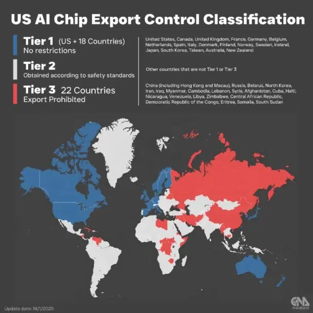
US semiconductor exports operate on a three-tier system: Tier one includes countries like the United Kingdom, France, and most EU nations, where high-end AI compute chip exports face minimal restrictions. Tier two encompasses countries like India — considered close partners but not fully trusted. AI compute exports to tier-two nations are highly regulated, with an apparent annual cap of approximately 100,000 AI chips per nation.
Tier three comprises countries like Russia and China, facing severe export restrictions or outright denial of AI chip access. As India's economy grows and geopolitical dynamics shift, these restrictions could potentially tighten, with the worst-case scenario being relegation to tier-three status.
The AI industry's overdependence on NVIDIA compounds this vulnerability. NVIDIA's integrated ecosystem of hardware and software makes it relatively straightforward for users to train and deploy AI models at scale. As the primary supplier, NVIDIA maintains massive order backlogs, with well-funded US companies holding priority positions.
Countries like India inevitably fall into secondary customer categories. Moreover, NVIDIA chips weren't originally designed specifically for AI computation — unlike contemporary alternatives like Google's TPU v4. The AI-capable tensor cores coexist alongside traditional vector cores, creating efficiency compromises, yet demand remains overwhelming.
When facing potential restrictions, nations confront two paths: capitulation in the AI race or innovation born of necessity. This convergence of compute scarcity and restricted chip access illuminates a fundamental requirement: India must build its semiconductor industry to achieve sovereign compute capabilities.
Learning From China: Innovation Through Necessity
China provides a compelling example of innovation born from necessity. Due to US export restrictions, China has invested heavily in domestic semiconductor capabilities, understanding that without a strong domestic semiconductor tool industry, building powerful AI models remains impossible.
The Chinese government anticipated the US-led Western semiconductor industrial tools blockade and incentivised domestic firms accordingly. Companies like Shanghai Micro Electronics Equipment (SMEE), Advanced Micro-fabrication Equipment Corporation (AMEC), and Naura Technologies now produce semiconductor manufacturing equipment, while firms like Empyrean Technology, Xpeedic Technology, and Primarius provide essential EDA tools comparable to Siemens and Cadence.
These developments are backed by China's semiconductor industry-specific 'Big Fund,' which has invested over $130 billion in domestic semiconductor companies. The latest iteration, Big Fund 3.0, launched in 2024, embraces a dual approach targeting both the entire semiconductor supply chain and specific critical areas, fostering growth across design, manufacturing, packaging, testing, equipment, and materials.
China's domestic tools receive rapid feedback from strategic companies like Semiconductor Manufacturing International Corporation (SMIC), Huawei, and Yangtze Memory Technologies Corporation (YMTC). This creates rapid iterations and continuous improvement. China is actively pursuing cutting-edge Extreme Ultraviolet Lithography (EUV) tools, taking innovative approaches like developing EUV mirrors through space-based solar X-ray imaging projects.

Chinese companies like Huawei, with its Ascend series chips, and startups like Moore Threads and Lisuan, developing next-generation GPU chips, are now considered just one generation behind NVIDIA. Due to geopolitical tensions and increasing competition, however, this specific approach may not be directly viable for India.
India's Strategic Path Forward
The Multi-Pronged Approach: India's approach to building a sovereign semiconductor ecosystem should encompass the entire supply chain — from design tools to fabrication equipment to inspection systems — while simultaneously developing the skilled workforce needed for this sophisticated industry.
The current Indian government's Design Linked Incentive (DLI) scheme resembles China's 'Big Fund' superficially but suffers from critical drawbacks. The DLI lacks clearly stated goals, presents overly general problem statements that highlight insufficient technical depth, and often produces only laboratory projects without commercial viability. Most critically, the India Semiconductor Mission focuses primarily on chip fabrication while neglecting the machine tools needed to design and manufacture chips from the ground up.
Building the Talent Foundation: The semiconductor manufacturing ecosystem divides into three categories: design (using computer-based tools to create digital chip designs), fabrication (manufacturing designed chips onto silicon wafers), and inspection (verifying fabricated chips match original designs).
India possesses significant advantages in talent development. Unlike China's early 2000s starting point, today's knowledge landscape is more democratised and accessible. The Indian government, students, researchers, and startups should capitalise on this opportunity.
The Design Pathway: For semiconductor chip design, several key components matter: base-level architecture enabling proper chip function, design tools converting architecture into machine-readable formats, and optical photolithography simulation tools modelling chemical and light pattern interactions.
Students can begin with GPU architecture fundamentals, given the high demand for general-purpose GPU chips and ASICs (application-specific integrated circuits) in AI and HPC (high-performance computing) workloads. OpenLane provides a comprehensive open-source chip design platform integrating tools like Yosys for RTL synthesis, OpenROAD for placement and routing, Magic and Netgen for layout verification, and KLayout for GDSII visualisation.
Open-source GPU and ASIC architectures (here and here) exist for educational purposes. Notably, Adam Majmuder, an Indian-origin student, has compiled complete GPU design learning materials in a freely available GitHub repository.
For computational photolithography, open-source tools like LithographySimulator, Optolithium, and OpenILT can simulate chemical-light interactions and predict pattern outcomes. These tools divide into computational photolithography (predicting how digital photomask designs appear on physical wafers) and inverse lithography tools (modifying photomask patterns for near-perfect physical printouts).

Strategic Problem Statements: The government should incentivise students and researchers through clearly defined problem statements, such as:
Design of computational photolithography simulators with inverse lithography functions and machine learning acceleration
Universal chip architecture with supporting software stacks for machine learning algorithms
Language model-based generative design features for photomask generation
End-to-end integrated chip design and verification tools with ML-accelerated workflows
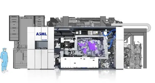
Fabrication Tool Development: Lithography machines represent the most prominent fabrication tools, comprising multiple high-precision subcomponents: mirrors, lenses, light sources, photomasks, scanners, precision lateral movement stages, and pressure regulators. The most cutting-edge machines are ASML's EUV lithography systems, featuring three critical components: a light source, high-precision mirrors, and wafer handling stages.
India should leverage existing expertise within government research institutes. The Bhabha Atomic Research Centre (BARC) possesses relevant capabilities for EUV light source development. BARC's Accelerator and Pulsed Power Division, led by Dr Amitabha Roy, has extensive experience with soft X-rays and related subsystems. EUV light falls within the 10-100 nm band of soft X-rays, and Dr Roy has authored research papers on molten tin-based EUV light generation.
The laser source for heating tin droplets could be developed as a DRDO fibre laser technology spinoff. For EUV mirrors, China developed theirs through their space agency as a solar soft X-ray imaging telescope project spinoff. India could achieve similar success through BARC's Atomic & Molecular Physics Division, which has long worked on multilayer mirrors for X-ray and neutron applications.
High-precision 2D positioning stages for nanometre-level wafer placement typically use magnetic levitation technology. Research from Dr P Ananthababu and Dr K S Vikrant demonstrates India's potential for developing high-precision maglev positioning stages, supported by various open-source projects available for student development (here, here, and here).
Inspection and Support Systems: Electron microscopy-based imaging techniques detect pattern shapes and defects in semiconductor manufacturing. Open-source projects exist for scanning electron microscopy (SEM) and transmission electron microscopy (TEM) development. These tools can be fabricated, tested, and improved through Indian academia and industry collaboration, with eventual commercialisation through government-supported startup ventures.
Various sputtering and vapour deposition tools, essential for semiconductor manufacturing and EUV mirror production, also have open-source project foundations that students and researchers can build upon (here and here).
A National Mission For Semiconductor Sovereignty
The current geopolitical scenario presents India with a unique opportunity to rewrite its semiconductor journey. All necessary tools are available — open-source technologies, talented diaspora, existing research capabilities, and growing industry demand.
The government must launch a comprehensive national mission involving Indian academia, scientists, engineers, MSMEs (micro, small, and medium enterprises), and startups. University-level students should be integral to this mission, creating a skilled workforce with hands-on understanding.
Talent Mobilisation: India must tap into its global diaspora of semiconductor experts, similar to China's early approach. Indian-origin scientists and engineers currently working for global semiconductor firms should be recruited as mentors or research team leaders. The government must individually reach out through targeted outreach programmes, offering opportunities to contribute to national technological sovereignty.
Collaborative Structure: A seamless collaboration framework should connect diaspora talent with India-based academicians, engineers, scientists, startups, and MSMEs, minimising bureaucratic hurdles that have historically discouraged top talent from contributing domestically.
Industrial Integration: The government must ensure sufficient chip design and fabrication firms serve as first customers for indigenous tools. Industrial feedback is essential for complete development and commercial deployment. Companies like Agrani Labs (developing GPUs in India), InCore Semiconductors, and the Tata-PSMC fab unit should work hand-in-hand with indigenous toolmakers.
Competitive Excellence: Open competition between teams should be encouraged, with freedom to fail recognised as essential to innovation. Adequate funding, clear problem statements, and defined end goals will drive success under visionary leadership.
Supply Chain Integration: The DLI mission must issue definitive problem statements to competing startups and companies, ensuring development of real-world useful products using indigenous semiconductor technology stacks.
Seizing the Moment
India stands at a crossroads. The convergence of geopolitical tensions, technological democratisation, and our substantial talent pool creates an unprecedented opportunity to achieve semiconductor sovereignty. The choice is stark: continue dependence on foreign supply chains that may become increasingly restricted, or embark on the challenging but essential journey toward technological self-reliance.
The compute bottleneck that threatens India's AI sovereignty can only be resolved through indigenous semiconductor capabilities. This requires not just political will and financial investment but a comprehensive national mission that harnesses our greatest asset — human talent — in service of technological independence.
The fire of AI burns bright in our time. India must not merely borrow this flame from others; we must kindle our own. The path is demanding, but the destination — true technological sovereignty in the AI age — makes every effort worthwhile.
The question is not whether India can build its semiconductor industry, but whether we have the collective will to begin this essential journey. The moment is now. The choice is ours.
Arpan Sow holds a Master of Science degree in Aerospace Engineering from Technion, Israel, and is currently a PhD candidate there. He is an avid aerospace propulsion and semiconductor enthusiast.
Get Swarajya in your inbox.
Magazine