Uttar Pradesh
Inside YEIDA’s Vision To Build A World-Class Electronics Hub At Jewar: An Interview
Ankit Saxena
Aug 20, 2025, 01:49 PM | Updated Sep 17, 2025, 07:33 PM IST
Save & read from anywhere!
Bookmark stories for easy access on any device or the Swarajya app.
India is aiming to scale up its electronics manufacturing ecosystem, with the objective of positioning the country as a global hub for Electronics System Design and Manufacturing (ESDM). The strategy focuses on increasing domestic value addition, exports, and attracting investments.
This is being supported through several government initiatives such as the National Policy on Electronics 2019 (NPE 2019), the Production Linked Incentive (PLI) scheme, and the development of industrial clusters under the EMC 2.0 scheme.
EMC 2.0 is designed to offer world-class infrastructure and encourage global electronics manufacturers and supply chains to establish a presence in India.
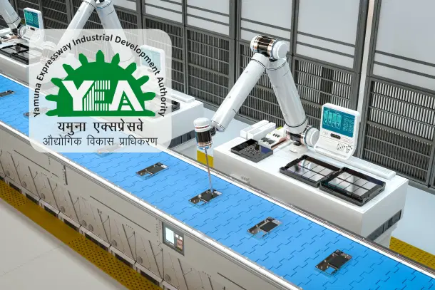
Under the scheme, the central government approved a Rs 417 crore Electronics Manufacturing Cluster (EMC) under YEIDA's jurisdiction in Sector 10. This cluster will support industries such as consumer electronics, automotive and industrial electronics, medical devices, computer hardware, and communication equipment.
It is expected to attract investments of approximately Rs 2,500 crore and create nearly 15,000 direct jobs.
To gain deeper insights into the vision of developing the electronic manufacturing cluster, Swarajya spoke with YEIDA’s IAS Shailendra Bhatia, who has been key in leading the development and strategic planning of this ambitious project for both the state and the nation.
Swarajya: What was the core inspiration behind establishing a world-class electronics manufacturing hub, and how does it align with Uttar Pradesh's broader industrial goals?
Shailendra Bhatia: Gautam Buddha Nagar, which includes Noida, Greater Noida, and the YEIDA region, has witnessed remarkable growth in electronics manufacturing over the years.
The area is already home to several prominent companies such as Dixon Technologies, Optiemus Electronics Limited, Havells India and Samsung Engineering. Yet there was no dedicated cluster to bring synergy, efficiency, and shared infrastructure to the sector.
This served as a major inspiration for the development of a world-class electronics manufacturing hub in the region.
The Government of India’s Electronics Manufacturing Cluster (EMC) 2.0 scheme in April 2020 provided an ideal opportunity for states to establish such focused industrial parks.
With increasing national attention on reducing dependence on imported components and enhancing domestic capabilities, the timing was right to invest in infrastructure that would attract manufacturers and strengthen the local value chain.
YEIDA took the lead by preparing a Detailed Project Report (DPR), leveraging its infrastructure, strategic location near the upcoming Noida International Airport, and alignment with both regional and state-level industrial development plans.
Electronics manufacturing, by nature, requires relatively compact space but yields high economic output. This makes it well-suited for integration into a high-density industrial ecosystem.
Moreover, the larger region under the authority is planned as a comprehensive industrial hub with parallel developments such as the Medical Device Park, the MSME and Apparel Park, and more. Setting up the electronics cluster here complements this broader vision, enhancing Uttar Pradesh’s manufacturing capabilities and its export potential.
S: Can you explain the scale and unique features of the proposed electronics cluster in Sector 10, especially the design aspects that set it apart from other industrial parks in India?
SB: The proposed cluster spans an area of 206.40 acres and is one of two such clusters approved under the EMC 2.0 scheme. One is in Tamil Nadu and the other is in YEIDA.
This will be the only dedicated EMC cluster in northern India, giving it a strategic edge in the region.
While there are various industrial areas engaged in electronics manufacturing, this cluster is unique in its focused, end-to-end ecosystem designed specifically for the electronics sector.
The cluster has been planned with both scale and adaptability in mind. Out of the total area, 105 acres have been planned into 66 industrial plots for companies interested in setting up manufacturing units.
Additionally, a 16-acre area, which is about 14 per cent of the saleable land, will feature Ready-Built Factory (RBF) sheds under a “plug-and-play” model. These flatted factory setups are ideal for start-ups and early-stage manufacturers who need fully equipped manufacturing spaces but may not have the resources to build their own.
The RBF units will come in various sizes, ranging from 60 to 120 square metres, catering to different operational needs. This flexibility is designed to lower entry barriers for smaller players.
Beyond the core manufacturing spaces, a three-acre Skill Development Centre will be developed. A two-acre Convention Centre will serve as a platform for industry networking, training, and exhibitions.
To support the workforce, the plan also includes 1.2 acres dedicated to hostel and accommodation facilities, making it easier for workers to live close to their workplaces. Additionally, 7.3 acres have been set aside for commercial use.
Sector 10 was chosen specifically for its proximity to the airport facility. The airport will feature a dedicated cargo terminal, and the cluster will be directly connected to the terminal within a 10-minute reach.
S: How does the proximity of the electronics hub to the upcoming Noida International Airport enhance its appeal for global and domestic investors?
SB: As the airport is being developed to be the largest in India, its advanced infrastructure will have a transformative impact on regional logistics and industrial development.
In addition to its passenger terminals, the airport will feature a multimodal cargo hub (MMCH), spread across 80 acres. This facility is designed to function as both a trans-shipment centre and a warehousing zone for freight forwarders and logistics integrators.
It will support multimodal transport operations, facilitating seamless transitions between road-to-road, road-to-air, and air-to-road movements.
The airport's dedicated cargo handling infrastructure is set to play a central role in shaping the future of the region’s supply chain ecosystem. Its close location to the airport brings a major logistical advantage.
Efficient air cargo will enable faster and more reliable movement of goods. This is a critical factor in the electronics industry, which thrives on speed, precision, and global integration.
The synergies between the electronics hub and the airport’s cargo facilities will create an integrated ecosystem conducive to high-volume and high-value manufacturing.
For electronics firms looking to scale operations, reduce lead times, and maintain global standards, this close proximity offers a strategic edge.
S: What other key infrastructure corridors will facilitate the growth of this industrial cluster?
SB: Adding to the air connectivity, expressways, freight corridors, and high-speed rail systems are being developed for the movement of goods, people, and services. This will further enhance the cluster’s competitiveness.
Road connectivity remains one of its greatest advantages, as the region is situated along the 165-kilometre access-controlled Yamuna Expressway. It connects directly with the Eastern Peripheral Expressway through a dedicated interchange, offering smooth access to the wider Delhi-NCR region.
Moreover, the expressway also ties into the Delhi-Mumbai Expressway via Faridabad, thereby linking the area to one of India's most important national logistics corridors.
Within the state, the Yamuna Expressway is integrated into Uttar Pradesh’s expanding expressway network, and further connects to the Agra–Lucknow Expressway, which extends to the Purvanchal Expressway. This creates a continuous corridor that spans the entire length of the state from west to east.
In addition to road infrastructure, the region is set to benefit from significant rail-based freight developments.
The proposed freight corridor is part of the Uttar Pradesh government’s plan to link Noida airport with the Delhi-Howrah main line near Chola station, and the Delhi-Mumbai line near Rundhi station.
The dual connectivity will provide the region with direct access to both eastern and western railway corridors.
Furthermore, the proposed Delhi–Varanasi bullet train corridor will pass through the region, with a dedicated station planned at the airport. Once operational, this line will reduce the travel time between Delhi and the region to just 21 minutes.
While the high-speed rail corridor is designed to provide long-distance connectivity, a Regional Rapid Transit System (RRTS) is also being planned to enhance regional mobility. This will enable the workforce from surrounding high-density areas to easily access the region.
S: How will anchor tenants like Havells and other major companies shape the ecosystem of this industrial cluster, and what will be the overall economic and social impact including job creation and skill enhancement for the local workforce?
SB: As one of India’s leading electrical goods manufacturers, Havells brings not only financial investment but also industrial credibility, technical know-how, and a well-established supply chain to the region.
The company has been allotted a 50-acre plot within the cluster, with an investment of Rs 800 crore in building its facility. This facility alone is projected to create at least 1,000 direct jobs.
Havells’ presence will likely encourage component manufacturers, logistics partners, packaging companies, and technology vendors to co-locate within or around the cluster.
In addition to Havells, several other large manufacturers with existing facilities in the Noida-Greater Noida region have expressed strong interest in expanding operations into this specialised EMC.
These companies are in various stages of planning, which shows the growing attractiveness of the cluster.
It is estimated that the entire cluster could generate close to 15,000 direct jobs and even more indirect employment opportunities. The sector will largely involve employment for skilled workers.
A major strength is also the alignment with the regional educational facilities. Gautam Buddha Nagar has also emerged as an educational hub, and its knowledge parks host over 200 academic institutions.
These institutions produce graduates in engineering, IT, and management, which are directly relevant to the electronics manufacturing sector.
With industry-academia collaborations on the rise, the proximity of these institutions offers a ready talent pool for companies coming up in the cluster.
Moreover, the dedicated skill development centre planned within the cluster will ensure sector-specific workforce training.
Overall, the EMC is designed to function as an ecosystem where infrastructure, industry, and human capital come together.
S: How will the Electronics Manufacturing Cluster (EMC 2.0) scheme and government incentives make this project both feasible and competitive globally?
SB: The central goal of EMC 2.0 is to enable the development of world-class industrial infrastructure by offering financial assistance to states and industrial development authorities.
This support is directed toward the creation of not just manufacturing clusters, but also Common Facility Centres (CFCs) that offer shared resources such as testing labs, logistics hubs, research facilities, and skill training institutes.
The scheme’s vision is not just about infrastructure but also about building a complete ecosystem.
The guidelines have defined the scope and structure of the EMCs, which has helped align the project with national objectives.
Moreover, the Ministry of Electronics and Information Technology (MeitY) has also ensured knowledge exchange, planning support, and policy guidance that have shaped the vision of the cluster.
The total funding for the project includes nearly Rs 145 crore as central financial assistance. YEIDA will provide Rs 393 crore toward the development of the cluster.
This joint investment is being used to build roads, services such as water and power supply systems, effluent treatment facilities, plug-and-play manufacturing sheds, and other key infrastructure elements that are vital for a globally benchmarked industrial hub.
With all these enablers coming together such as strategic location, infrastructure, financial incentives, and policy support, the cumulative impact is expected to surpass initial projections.
S: What are the major milestones and timelines for the project, and what steps have been taken to avoid typical roadblocks faced by large infrastructure developments?
SB: The project is expected to be completed within a 30-month window, beginning in July 2025.
During this period, all necessary infrastructure such as roads, power and water supply, common facility centres, and ready-built factory (RBF) spaces will be constructed and made operational.
The timeline also includes the full development of the ecosystem to support industrial units, logistics services, and workforce accommodation.
One of the key reasons the project is expected to avoid common roadblocks that are often faced by large infrastructure initiatives in India is the streamlined governance structure.
The entire planning and execution process is being managed by YEIDA, which serves as both the regulatory and implementing authority.
From land allotment and bidding to approvals and transfers, all processes fall under YEIDA’s jurisdiction. This eliminates the delays usually associated with dealing with multiple government departments and agencies.
By consolidating all critical functions under one authority, the project has improved the ease of doing business. Investors and manufacturers can handle the setup process smoothly, with fewer procedural obstacles, which will also enhance their confidence.
Get Swarajya in your inbox.
Magazine