Economy
#FabInIndia: Why The Government Must Act Now
- If expression of interest scheme-letter of intent is the government’s route for #FabInIndia, it must act fast and firm.
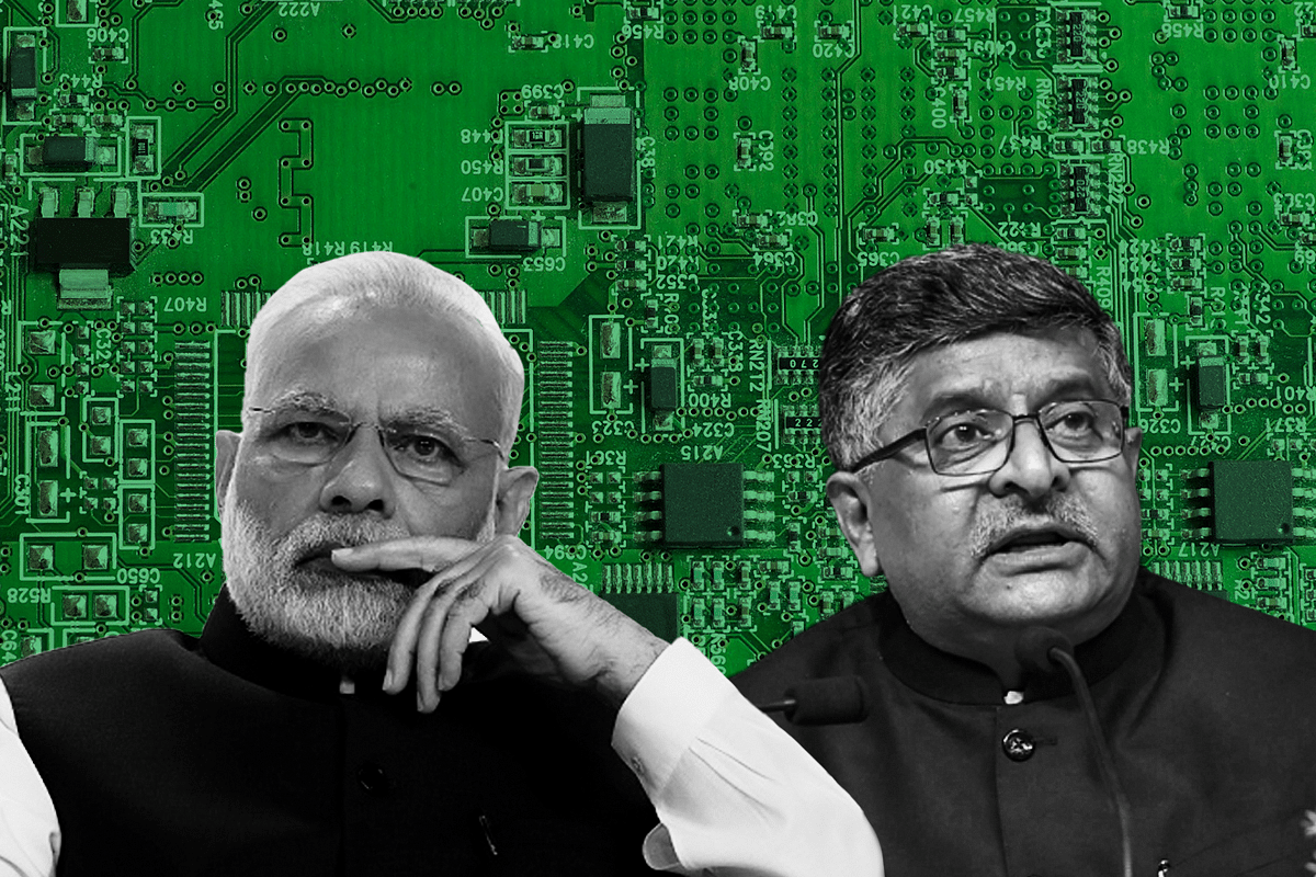
Prime Minister Narendra Modi and Minister Ravi Shankar Prasad.
On 9 October 2013, the then UPA (United Progressive Alliance) government through its Department of Electronics and Information Technology (DeitY) under Ministry of Communications and Information Technology issued this invitation of expression of interest (EoI) for setting up semiconductor wafer fabrication (Fab) facility in India.
The initial deadline was within four weeks, which was later extended to 25 November 2013 — in short, about 48 days were given. The parameters looked as follows:
Note that only "Advanced CMOS" was listed, a minimum of 40,000 wafer starts per month (WSPM) capability and a 300mm wafer size was asked for — all in a seemingly ‘must-be’ fashion as opposed to a ‘preferred’ fashion. Also, I did not see analog or other kind of fabs mentioned in that document. Among the key incentives offered included:
i. Incentives to the extent of 25 per cent of the capital expenditure of the project
ii. Subsidy of 25 per cent on growth capital expenditure
iii. Countervailing duty (CVD) on purchase of capital goods may be reimbursed
iv. Excise duty paid on the products of the Fab may be reimbursed for a period of 10 years and more, all subject to conditions in the policies of that time.
Did It Work? If Not, Why?
Rest of the story is summarised in an answer from the ministry to a question raised by MP Rajeev Chandrashekhar in Rajya Sabha on 11 July 2019, which is available here.
Based on the recommendations of the Empowered Committed (EC) constituted for the purpose of setting up of Semiconductor Wafer Fabrication (FAB) manufacturing facilities in the country, Government had approved two proposals for setting up of Semiconductor Wafer Fabrication (FAB) facility in India - one from the consortium led by M/s. HSMC Technologies India Pvt. Ltd. (with ST Microelectronics and Silterra Malaysia Sdn. Bhd. as partners) and the other from consortium led by M/s. Jaiprakash Associates Ltd. (with IBM, USA and Tower Semiconductor Limited, Israel as partners). Letter of Intent (LoI) dated 19.03.2014 were issued to both the consortia.
As per the LoI, both the consortia were required to submit the documents for demonstration of commitment. The consortium led by M/s. Jaiprakash Associates Ltd. withdrew their proposal on 02.03.2016, inter-alia conveying that the exchange rates in US $ / ? term has gone up by about 12% already over the last two years, even before the commencement of physical implementation, adversely affecting the total capital outlay for the project. Additionally, M/s. Jaiprakash Associates Ltd. conveyed that the viability of the project became questionable due to prevailing conditions in the country and the global scenario which indicated that the trend was likely to continue in the same pattern.
As regards the consortium led by M/s. HSMC Technologies India Pvt. Ltd., they could not submit the requisite documents for demonstration of commitment, as per the LoI, despite being provided extension of time on multiple occasions. Therefore, LoI issued to the consortium led by M/s. HSMC Technologies India Pvt. Ltd. was cancelled on 20.04.2018.
Notice that the ‘LoIs’ were issued 19 March 2014, by the UPA government just days before the first phase of general elections. Some questions do arise — were the parameters too stringent and inflexible for a first time commercial fab-in-India? Did the UPA government time the ‘EoI’ such that the ‘LoI’ and hence the media publicity could happen just before the elections? I don’t really mind if that eventually culminated in #FabInIndia , but I wonder if that was a ‘pass the buck’ move from UPA?
I tend to think that the UPA government would not have come up with such a pre-election move, with less than two months to apply, without having hints that at least some players would apply — especially given that the eventual applications were both in the form of consortiums involving multiple companies.
However, whether the fault of the government at that time or not, was it the right mix of players that came together? IBM for example, went fabless soon after, completing the sale of its fabs to GlobalFoundries by July 2015. The non-technical players involved too, were not very convincing. Tower Semiconductor is one group from which I still have hopes though.
After A Four-Year Wait By NDA-2014, Another Two Years Of Talk, Study, But No Action Followed
Fast forward, after seemingly waiting for nearly four years for the parties who were issued ‘LoI’ to essentially ‘go find investors’, and then ending up nowhere by 2018, what has the NDA (National Democratic Alliance) government done after that? I will be happy to be corrected, but I am afraid not much was done by NDA for the next two years either, apart from a mention in the first budget speech of the current Finance Minister in 2019, question-answer in Rajya Sabha quoted earlier and perhaps initiate this Indo-Israeli feasibility study in 2018 which came up with a detailed report in December 2019 with recommendations as follows, but I have not seen any comments on this from the ministry, let alone action.
An analogue and mixed-signal foundry at a technology node of 45/65 nm, could be a starting point for India to develop a semiconductor fabrication industry. Israel as a technology partner could transfer the initial technology, provide support to set-up the fab and support early market development. ... Monetary and non-monetary support will be needed from the Government of India, to attract investment in the proposed India fab. As per the financial model in the report, a cash subsidy of US$ 912 Mn on capex and an interest-free loan of US$ 1,089 Mn, could help achieve 15% equity IRR, the likely threshold for corporate investors.
Renewed Interest With The Atmanirbhar Bharat And Make In India Pitch
Things started to move a bit when in June 2020, through SPECS scheme, 25 per cent reimbursement on capex was offered. However, to the best of my knowledge, no one has applied for the scheme. Some of the clauses of the scheme — for example “Only 20% of the refurbished equipment will be considered for Capex subsidy” and only a small overlay which itself is shared money to subsidise other segments also- could have possibly dampened the interest.
There have also been rumours of the possibilities of the government coming up with an exclusive fab policy with 25 per cent reimbursement upfront, another 25 per cent after production starts and an additional, up to 25 per cent interest free loan as required — and this would have put anyone interested into a waiting mode, making the SPECS offer of no use.
All these and more importantly what kind of technology nodes should perhaps India target to start with, and various other topics have been dealt with in my series of articles in Swarajya , news4masses and orfonline — altogether 14 till date excluding this one.
In particular, this article in a nutshell argues that "It may be more practical and time critical to start with an analog or an analog/mixed signal fabs first, which also play a key role from a security perspective" and that such a fab or fabs will be “relatively lower investment as the technology nodes needed are still in 130/180nm or at best 45nm/65nm, greater return on investment (RoI) and yet, will demonstrate commercial semiconductor fab capability for India”.
If there are multiple players interested, or if one group is interested in more or future expansion I wish that a cluster of five types of fabs could be an eventual goal, including a 28nm digital and a possible niche III-V (ie compound semiconductor based) — all along, emphasising “India should stand up first, then walk, then run”.
What Is The Latest Move By The Government If India?
Come 15 December 2020, the ministry issued notice inviting EoI for setting up/expansion of existing semiconductor wafer/device fabrication (FAB) facilities in India or acquisition of semiconductor FABs outside India. The last date for submission of EoI proposal is 31 January 2020 —Swarajya reported on the same here.
How is it different, if at all, from the 2013 invitation for EoI ? Here are some points that I noticed based on a first read.
1) There is analog mentioned, and when it comes to tech-node and capacity (WSPM) suggestion, there is the word "preferably" — that will be key, given that if it is analog centric fab, even the ‘advanced’ ones will be 65nm or 45nm and even 130nm or 180nm would be good enough for a start in India — lots of data have been provided in my articles.
2) There is a category for III-Vs or any similar futuristic technologies.
3) There is a Category C too saying “Indian Companies / Consortia interested in acquisition of Semiconductor FAB outside India”. While that is not really "Make-In-India", I feel that it is surely good to have such an option given the time criticality and given the fact that there are Indian businessmen capable that, and eventually it could lead to opening #FabInIndia by the same group.
4) Perhaps the most important difference this time is this statement — "The information received in response of this EoI may be utilized to formulate a Scheme for setting up / expansion of existing Semiconductor wafer/device fabrication (FAB) facilities in India or acquisition of Semiconductor FABs outside India".
In my latest article towards the end of the July-September quarter, I had quoted a picture from a government document which gave hopes that the exclusive fab policy(scheme) that minister Ravi Shankar Prasad had claimed to be in the making, will come out before 2020 ends. Instead, the invitation of EoI seems to be almost like "back to square one".
However, perhaps — and I can only hope — it shows willingness from the government side to listen to interested parties on exactly what kind of hand holding they need. The document specifically asks the interested parties to detail the "Financial support desired from the Government of India, including Grant-in-Aid (GIA), Viability Gap Funding (VGF) in the form of Equity and / or Long-Term Interest Free Loan (LIFL), tax incentives, infrastructure support, etc".
Time is of essence here, especially in a scenario where China is going all out to boost its semiconductor fab capability and inviting various companies. Even with the sops pre-defined, it took the UPA government nearly four months after the EoI deadline of 25 November 2013 to issue the LoI to two consortiums. Going by that kind of timeline, assuming this government sticks to the EoI deadline of 31-January 2021 and that one or more parties will apply by then, given that it will need time to study the "request for desired financial support" coming from various parties, possible issue of LoIs look well into the second half of 2021, and if all goes well, a 2023 test-ready and 2024 production ready fab.
For anything to happen, the key factor remains that investors or groups have to come forward soon. With a renewed interest in the area of semiconductor chip manufacturing, globally and with governments and companies — especially in the US, China and South Korea — giving a lot of emphasis on boosting local manufacturing units, I hope Indian investors or groups will stand up too. Time alone can tell whether government already has a hint of someone interested or if this is just a "buy more time" move.
At this point we may have to console ourselves saying "something is better than nothing" and that "a country which has waited for 20 years can wait for four more years” — provided it does take off this time. Until commercial #FabInIndia takes off, #MakeInIndia cannot be considered all-encompassing in the electronic sector.
Support Swarajya's 50 Ground Reports Project & Sponsor A Story
Every general election Swarajya does a 50 ground reports project.
Aimed only at serious readers and those who appreciate the nuances of political undercurrents, the project provides a sense of India's electoral landscape. As you know, these reports are produced after considerable investment of travel, time and effort on the ground.
This time too we've kicked off the project in style and have covered over 30 constituencies already. If you're someone who appreciates such work and have enjoyed our coverage please consider sponsoring a ground report for just Rs 2999 to Rs 19,999 - it goes a long way in helping us produce more quality reportage.
You can also back this project by becoming a subscriber for as little as Rs 999 - so do click on this links and choose a plan that suits you and back us.
Click below to contribute.
Latest