Tech
Applied Materials Seeks To Challenge ASML's Dominance Of EUV-based High-End Semiconductor Chipmaking With Two New Products
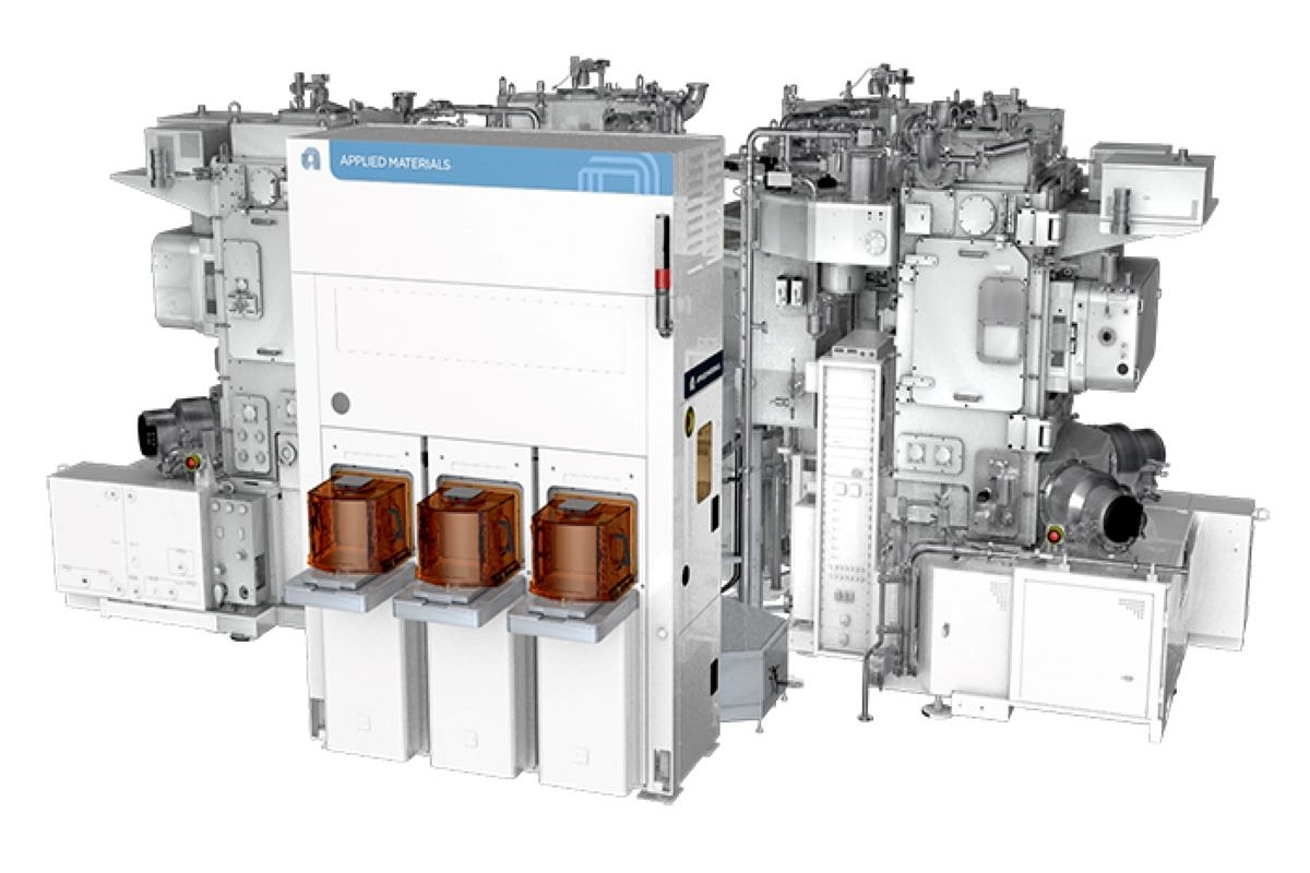
Applied Materials's Centura Sculpta system
Applied Materials is now offering two new semiconductor manufacturing tools in a bid to challenge ASML, the industry leader currently dominating high-end chip making using extreme ultraviolet, or EUV, lithography equipment.
Last week, Applied Materials unveiled two new products - the Centura Sculpta system that it says will provide a simpler, faster and more cost-effective alternative to EUV double patterning and VeritySEM 10 system to enable precise measurement of the dimensions of semiconductor device features patterned with EUV and emerging High-NA EUV lithography.
Lithography has become increasingly complex and expensive, and the new approach would help streamline chip production while reducing waste, Applied Materials said.
Applied Material added that the breakthrough in patterning technology would allow chipmakers to create high-performance transistors and interconnect wiring with fewer EUV lithography steps, thereby lowering the cost, complexity and environmental impact of advanced chipmaking. It will also eliminate a second step in the EUV chip manufacturing process called double patterning.
"Chipmakers can now print a single EUV pattern and then use the Sculpta system to elongate the shapes in any chosen direction to reduce the space between features and increase pattern density. Because the final pattern is created from a single mask, design cost and complexity are reduced, and the yield risk from double-patterning alignment errors is eliminated." the company said.
ASML Dominance To Be Challenged?
Applied Material's Centura Sculpta platform may threaten ASML's dominance of the lithography market as it will provide significant cost savings and speed up production for chipmakers producing leading-edge chips.
ASML, which enjoys a near monopoly on advanced EUV lithography equipment (Japanese competitors like Canon have a minuscule market share), is a crucial supplier to chip manufacturing giants including Intel, Samsung Electronics Co. and Taiwan Semiconductor Manufacturing Co (TSMC).
ASML's EUV-based machines use light to etch ultra-small circuitry on chips, allowing packing more performance into the small slices of the silicon wafer. The machines can emit light with wavelengths one-fifteenth as small as the conventional chipmaking equipment, enabling it to etch finer circuits and thus squeeze more transistors onto a chip. The patterns link together as a single integrated circuit offering computing or memory functions.
Founded in 1984 as a joint venture between the Dutch companies Advanced Semiconductor Materials International (ASMI) and Philips, ASML began working on the EUV system in 1997
The EUV machine took decades to develop and was introduced for high-volume manufacturing in 2017. the machines are some of the most expensive in the industry and cost more than $150 million. Shipping it to customers requires 40 shipping containers, 20 trucks and three Boeing 747s.
ASML’s approach has few drawbacks. Some parts of the chip require what is called multiple patterning — taking two or more runs through the process to achieve the desired results.
Support Swarajya's 50 Ground Reports Project & Sponsor A Story
Every general election Swarajya does a 50 ground reports project.
Aimed only at serious readers and those who appreciate the nuances of political undercurrents, the project provides a sense of India's electoral landscape. As you know, these reports are produced after considerable investment of travel, time and effort on the ground.
This time too we've kicked off the project in style and have covered over 30 constituencies already. If you're someone who appreciates such work and have enjoyed our coverage please consider sponsoring a ground report for just Rs 2999 to Rs 19,999 - it goes a long way in helping us produce more quality reportage.
You can also back this project by becoming a subscriber for as little as Rs 999 - so do click on this links and choose a plan that suits you and back us.
Click below to contribute.
Latest