Tech
Exclusive Interview: Sahasra Semiconductors’ CTO Talks Chip Packaging Plans In India
- Sahasra Semiconductors is a newly formed entity under Sahasra Group with a mission to start semiconductor assembly and testing in India.
- Read our interview with the company's Chief Technology Officer Shiv Kumar about their plans.
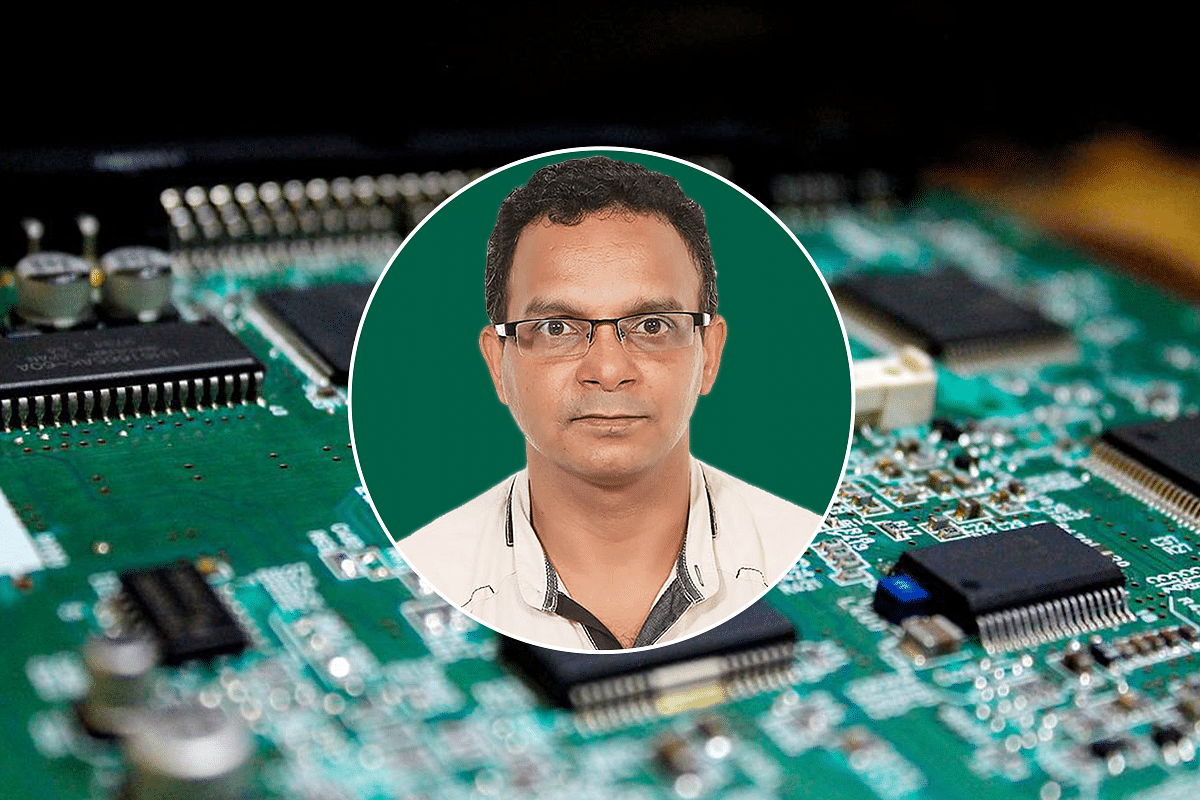
Shiv Kumar is Sahasra Semiconductors' Chief Technology Officer.
It came to light recently that Rajasthan-based Sahasra Semiconductors Private Limited (SSPL) plans to invest Rs 750 crore in setting up a memory chip assembly, test, and packaging unit in Bhiwadi.
In its report, for which the news agency spoke to the company’s chairman and managing director Amrit Manwani, PTI said SSPL expects to become the first company to set up such a unit in India and would begin selling locally made (tested/packaged) chips by the year-end.
Sahasra Semiconductors is an emerging semiconductor company in India with a focus on chip packaging. In an email interview with Swarajya contributor Arun Mampazhy, the company’s Chief Technology Officer Shiv Kumar shared some of their updates and plans for the future.
Kumar holds a Master’s degree in Materials Science from the Indian Institute of Technology (IIT), Kanpur, and has worked in Sandisk (Shanghai, China) and Semtech Corporation (Shanghai and the United States).
He has 14 years of experience in semiconductor packaging (wire bonding, wafer-level packaging, 2.5D/3D packaging, bumping, through silicon vias, etc), testing, fabrication, and business development.
Here are the edited excerpts from Mampazhy’s interview with Kumar.
Q. Please give us a brief history of SSPL. Who are the key people who came together and what was the motivation?
SSPL is a newly formed entity under Sahasra Group with a mission to start semiconductor assembly and testing in India. Mr Amrit Manwani (CMD, Sahasra Group) wants to begin real semiconductor manufacturing in India that has been missing till now. The other key group is Desai Electronics Pvt Ltd.
Since Sahasra Group has been in the memory business for the last five or more years, we have planned to start assembly and test for memory chips. We are also planning to add assembly and testing for LED driver chips in the future.
Q. The SSPL website says that the company was incorporated on 15 July 2020. So, it has been about two years. Please tell us in brief what have been the key updates so far? Is the company focused on assembly and testing only for products it will market, or also as a service?
The building and clean room are ready and purchase order of all major tools are in place. We are planning to have low-volume production by Q1 2023.
We are going to be a manufacturing house that will provide both Outsourced Semiconductor Assembly and Testing (OSAT) services for others as well as Assembly, Testing, Marking, and Packaging (ATMP) for ourselves.
(Mampazhy’s Note: On their website, it says the “Company is India’s first and only private company to start NAND FLASH IC packaging and testing operations… coming up at Bhiwadi, Rajasthan…”
Q. Is this facility being set up with incentives via the PLI (Production-linked Incentive) and SPECS (Scheme for Promotion of Manufacturing of Electronic Components and Semiconductors) schemes (announced in June 2020)? Can you tell us a bit more about exactly what kind of proposals from SSPL have been approved under these schemes? Who are the investors?
Sahasra Semiconductors has obtained approval of the PLI, SPECS, and customised incentive from the state government for NAND Flash Memory packaging and testing.
We are on target to start manufacturing (Q1 2023). SPECS does not include incentives for building construction costs. Also, PLI will give incentive only upon meeting sales targets set by the government, based on investment values. Major investors are Sahasra Group and Desai Electronics Pvt Ltd.
Q. How different are the new schemes for ATMP/OSAT launched in December 2021 by India Semiconductor Mission (ISM) along with the schemes for semiconductor and display fabs?
The latest released scheme by ISM offers 30 per cent incentive compared to 25 per cent on Capex offered by SPECS. New scheme by ISM is specially dedicated to boost semiconductor manufacturing, since it covers not only capital but other expenses too.
More rounds of PLI schemes are also announced with the same rules as initial ones, but we would like to see some changes in PLI. Since semiconductor manufacturing is a three- to four-year process, in order to reach the level where a product comes out of the factory (building construction to mass-production readiness), the PLI should be counted from the date of manufacturing start instead of from the date of approval letter.
Q. Why did SSPL start with NAND FLASH IC packaging? Is this being offered as its own product or also as service for other companies? How is the customer response so far?
As I mentioned earlier, Sahasra is involved in assembling chip-on-board (COBs) and solid state drives (SSD) for memory, in which NAND Flash ICs are used and, hence, Sahasra is planning for NAND Flash IC packaging.
We are talking to all major memory suppliers and we got positive feedback from them. For our own brand, we have discussed our products with end customers for applications such as mobile phone, IoT (internet of things) devices, home gateway devices, automotive, data server, and data centres.
The LED driver packaging, which is in the pipeline for extension, will also be our first product that will be completely designed, developed, and assembled in India (except the fabrication).
Q. In my interview with Raja Manickam, the CEO (chief executive officer) of Tata Electronics (OSAT division), in response to a question (No 4), he had mentioned about mature technology in packaging, which is relatively easier, and advanced technology (heterogenous packaging), which involves more. What are your views on this and where do you place SSPL? From what is known so far, will the Tata OSAT efforts overlap with that of SSPL, or are they different?
Twenty or more years earlier, packaging was thought to be only a protection for silicon, but, for the last one decade, it is getting more and more performance-driven. Hence, complexities are increasing even in mature technology.
New technologies are also on the way. What is needed and what is relevant depends on the applications. Some mature technologies will stay here for the next one or two decades because of demand and cost effectiveness.
Heterogeneous packaging is coming very fast due to chiplet introduction and higher output density requirement. They are more complex because of shrinking sizes, reducing form factors, etc. Flash memory still uses (and will continue to use) gold (symbol “Au”) wire bonding, which is matured, but as I said, due to a performance-driven approach, it is also not easy to build them at reduced bond pad opening, pitch, and die thickness.
Tata is most probably planning to move with advanced packaging products for very high-level applications. We do not have any overlap with them.
Q. How much emphasis is there for industrial R&D (research and development) within SSPL? What are your views on investments done in industrial R&D by Indian technology companies in general, and do you see SSPL being different from that?
SSPL will be focusing on research and development a lot. See, R&D is a major pillar in semiconductor manufacturing because you need to be ahead of your competitors or else you will be thrown out. The SSPL R&D team will work on different fronts, such as building new products from scratch, building products based on customer specification, and building products on market demand in such a way that makes SSPL products better than competitors.
Most of the global semiconductor companies spend 10-15 per cent on R&D alone. It is a must to invest in R&D. Many of the companies in India either do not invest at all or invest a small amount that keeps them vulnerable in the market. We will move away from this mindset.
Q. On 19 February 2021, when the government initially announced the names of the applicants under the Semicon scheme, there were four for OSAT/ATMP. There are indications that since then, the government has received some more applications, as the scheme is still open. In your opinion, how many small and large OSAT companies can India have? Also, any other comments on the government schemes and the way they are being executed?
Firstly, nobody can survive if they target only the Indian market, despite the fact that the Indian market is huge. We have to think global as well. But we have the leverage to start it for the local market first and then expand. To stay competitive in the market, we have to build high volume and it will take some time to reach there.
Secondly, we have to keep in mind that we do not have raw material (processed wafers) available domestically and it will not be available for the next at least eight to 10 years on a large scale.
Availability of processed wafers on a large scale is the backbone for OSATs due to multiple factors. Once we have the ecosystem, we can absorb 10-15 OSATs (small and big) in India.
As said, PLI needs to be adjusted if they really want to implement it.
Q. As closing remarks, any thoughts on other aspects of building the semiconductor packaging industry in India? For example, support from the states, how much talent building is needed, etc? With all these (factors), where do you see India in this space, say, by 2025 or 2030?
Governments need to start working quickly on building infrastructure (water, electricity, and transportation). Even though it is in the hands of the state government, the central government should coordinate and help. They should also start thinking about how to bring in other related industries such as raw material manufacturers (mold compound, adhesives, substrates, Si crystal growth, wires, etc), equipment manufacturers, production carriers (magazines, trays, tubes, reels, etc), and chemicals and gases in India to complete the ecosystem. They should give a chance to those who really know what semiconductor manufacturing is, call them, and discuss with them because they have hands-on experience.
We have enough talent in India, but we have to sharpen them for industries. The semiconductor industry is a totally different beast that needs a lot of attention every fraction of a second. For this, a smart and intelligent engineering force is required. Great incentives should be in place to retain this talent. A great management team with appropriate skills in the semiconductor domain will drive it faster than anybody else.
As for India’s positioning in this space in the near-future, there are plans, but many are still on paper. I believe that we will see initial results by 2027-28 (overall semiconductor manufacturing, construction of sites, associated small-scale industries, R&D, reliability activities, etc). To reach a comprehensive level, we need 20-25 years.
Mampazhy: Thank you, Mr Shiv Kumar, for your responses, and best wishes to SSPL in its exciting journey ahead.
Support Swarajya's 50 Ground Reports Project & Sponsor A Story
Every general election Swarajya does a 50 ground reports project.
Aimed only at serious readers and those who appreciate the nuances of political undercurrents, the project provides a sense of India's electoral landscape. As you know, these reports are produced after considerable investment of travel, time and effort on the ground.
This time too we've kicked off the project in style and have covered over 30 constituencies already. If you're someone who appreciates such work and have enjoyed our coverage please consider sponsoring a ground report for just Rs 2999 to Rs 19,999 - it goes a long way in helping us produce more quality reportage.
You can also back this project by becoming a subscriber for as little as Rs 999 - so do click on this links and choose a plan that suits you and back us.
Click below to contribute.
Latest