Tech
Extreme Ultraviolet Lithography: Will High Numerical Aperture Tools Be The End Of Decades-long Innovation?
- What does it mean when ASML CTO says "high-NA will be the last NA?"
- Here's the background you need to better understand it.
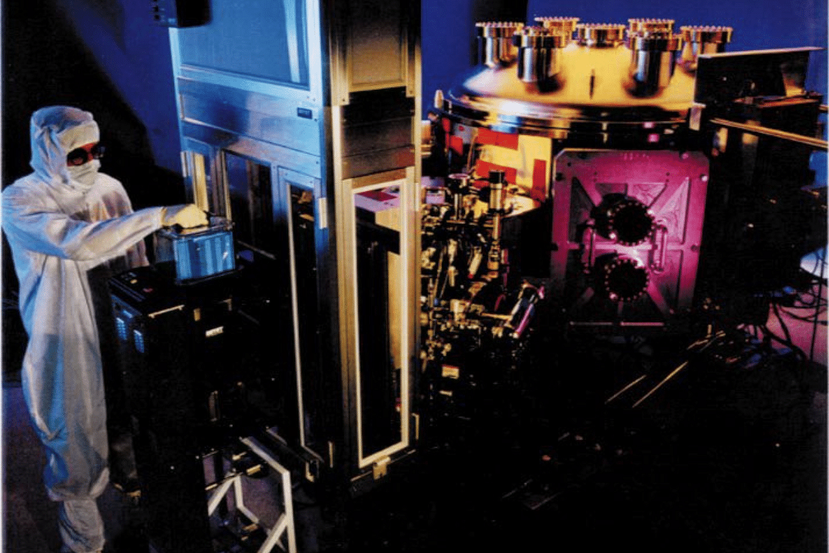
An extreme ultraviolet lithography (EUVL) tool (Photo: Lawrence Livermore National Laboratory/Wikimedia Commons)
"After decades of innovation in lithography, high-NA EUV might prove to be the end of the line."
This is how Dutch media company Bits&Chips summed up Martin van den Brink's insight on the progress of lithography innovation.
Van den Brink is the chief technology officer of the wafer fab equipment (WFE) maker ASML, which is based in the Netherlands.
Here's some background and context to make sense of the technical aspects surrounding his view.
But First...
Note that:
– ASML is one of several WFE makers. As per some analysts, ASML had about 20 per cent market share in 2021 and was slightly behind Applied Materials. Tokyo Electron Limited, Lam Research, and KLA are the other names in this category.
– WFE includes tools for a variety of process steps in a semiconductor chip fabrication plant (fab); for example, lithography, etching, deposition, diffusion, implant, chemical-mechanical polishing, and metrology.
– ASML is a leader in photolithography equipment and its offerings are usually among the costlier ones.
Background
A chip contains many "layers," such as the active area, the gate layer, contact, metals, and vias.
The design of each layer, after appropriate modifications for printability, are turned into photomasks.
Lithography in a fab (fabrication plant) involves printing patterns from the photomask to photoresist-coated wafers — usually tens or hundreds of wafers every hour.
Not all the layers will have the smallest dimension indicated by the technology node. For example, large-area implants and fat metals can have dimensions in micrometres.
However, some layers like the gate layers, contact, and first level of metal will have dimensions comparable to the technology node number.
The smallest feature size that a lithography tool can "resolve" (print) is:
– Directly proportional to the wavelength of the light source used
– Inversely proportional to the "numerical aperture" (NA) of the whole system, and
– Proportional to the "k factor," which depends on a variety of process factors and is usually "reverse calculated"
Usually laser-produced ultraviolet (UV) light is used as a source in lithography equipment known as stepper or step-and-scan tools.
Examples of "older"-generation source wavelengths are 365 nm and 248 nm. These tools are still used in fabs to print layers with not-too-small dimensions.
The 365 nm tool was useful for up to about 250 nm technology node and 248 nm tool for up to about 130 nm. For layers with smaller dimensions in technology nodes up to 65 nm (as well as for the "half-node" 55 nm), lithography tools based on 193 nm wavelength were useful. 248 nm and 193 nm falls under deep UV (DUV) of the spectrum.
In the 193 nm lithography tool, by adding a layer of water between the projection lens and the wafer, an NA close to 1.35 was achieved. This came to be called immersion lithography. It made 28 nm possible — perhaps even 22 nm with some other tricks.
For technology nodes below that, to print those layers with the smallest features, fabs started doing "multiple patterning" using the 193 nm immersion lithography tool itself. Up to 7 nm chips have been achieved using this technique.
All the tools mentioned so far have multiple manufacturers; though with increasing sophistication, the number of companies doing them have shrunk. Only ASML and Nikon make the 193 nm immersion lithography tool, while for the older-generation ones there are also ones like Canon.
Wavelengths below 193 nm started falling into the extreme ultraviolet regime (EUV), which created a big challenge — this light is absorbed by glass and even air.
It took ASML many years to develop practical lithography tools based on an EUV source. To date, ASML has a monopoly in this area.
Fabs started using 13.5-nm wavelength EUV-based lithography systems for high-volume chip manufacturing of advanced nodes only a few years ago. Samsung, for its 7 nm process node, was perhaps the first. TSMC soon followed with its N7+, and Intel is in the process of using them for Intel 4.
For an EUV-based lithography tool to be effective, the whole system has to be in a tight vacuum. Photomasks have to be reflective, and, instead of a lens system, you need a projection system based on extremely smooth mirrors.
For ‘standard’ EUV, NA is only 0.33. This offset some of the gain due to the smaller wavelength. ASML has been on a mission to try to increase this parameter. The next-generation 0.55 "high NA" tools are on the way.
It is said that 0.33 NA optics provides 13 nm resolution.
"This resolution is good enough for a single-pattern approach at 7 nm/6 nm nodes with 36 nm ~ 38 nm pitches and at 5nm with 30 nm ~ 32 nm pitches. But as pitches get below 30 nm (at beyond 5 nm nodes) the 13 nm resolution might call for dual lithographic exposure that is going to be used for years to come."
"Pitch" in the quoted text refers to the distance at which the minimum feature size pattern repeats itself.
The high-NA tool is expected to help avoid multi-patterning at 3 nm and beyond, but it is likely to bring additional challenges as well.
The anamorphic mirrors used in the tool will have an 8X magnification in one direction and 4X in the other, compared to the standard 4X magnification in all directions for tools used so far.
This will reduce the printable field in one direction into half, which could pose a challenge for chip designs larger than a certain size.
Points to note
With this context, here are some key points or quotes from the ASML CTO interview:
* Is another increase in NA a possibility? ASML is looking into it; that is, hyper-NA of about 0.75. But, personally, he doesn’t believe that hyper-NA will prove viable.
"We’re researching it, but that doesn’t mean it will make it into production. For years, I’ve been suspecting that high-NA will be the last NA, and this belief hasn’t changed," he said.
Also note that:
* A new step down in wavelength isn't an option, ASML’s Vice President of Technology Jos Benschop revealed at the SPIE Advanced Lithography conference last year.
That has to do with angles: the efficiency with which EUV mirrors reflect light depends strongly on the angle of incidence. A step down in wavelength would change the angular range such that the lenses (mirrors) would simply have to become too large to compensate.
The interview ends with these words from the ASML CTO: "For hyper-NA, we’re accepting that there may be an insurmountable cost constraint, not in the least because transistor shrink is slowing down.
"Thanks to system integration, it will still be worthwhile to keep developing new chip generations – that’s the good news. But at this point, the question has become very real: which chip structures are too small to manufacture economically?”
Support Swarajya's 50 Ground Reports Project & Sponsor A Story
Every general election Swarajya does a 50 ground reports project.
Aimed only at serious readers and those who appreciate the nuances of political undercurrents, the project provides a sense of India's electoral landscape. As you know, these reports are produced after considerable investment of travel, time and effort on the ground.
This time too we've kicked off the project in style and have covered over 30 constituencies already. If you're someone who appreciates such work and have enjoyed our coverage please consider sponsoring a ground report for just Rs 2999 to Rs 19,999 - it goes a long way in helping us produce more quality reportage.
You can also back this project by becoming a subscriber for as little as Rs 999 - so do click on this links and choose a plan that suits you and back us.
Click below to contribute.
Latest