Tech
Two New Developments At Semi-Conductor Laboratory: MeitY Seeks Two Key Roles For Mohali Lab
- The Semi-Conductor Laboratory is seeking two key appointments for its Mohali facility.
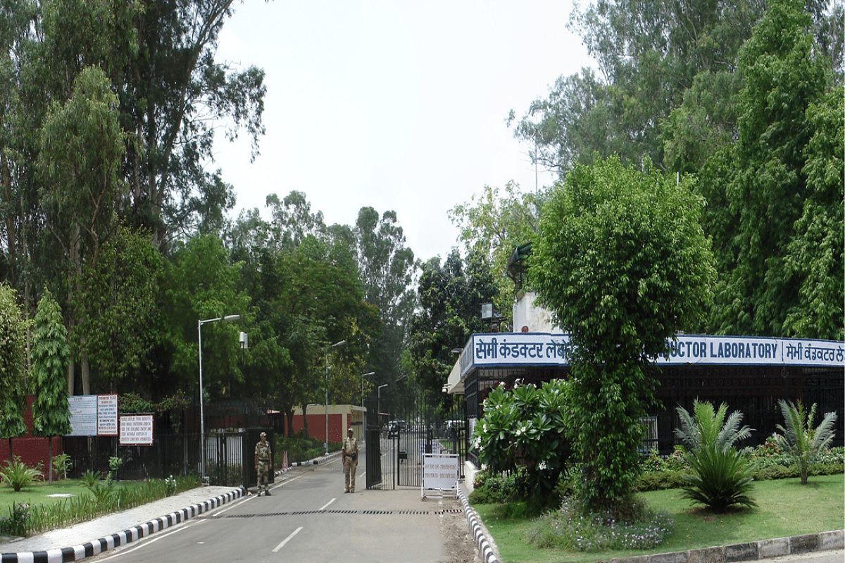
The main gate of the Semi-Conductor Laboratory
The Ministry of Electronics and Information Technology (MeitY) is on the lookout for a director to head the Semi-Conductor Laboratory (SCL) in Mohali, Punjab.
SCL is an autonomous institution under MeitY, Government of India, located in SAS Nagar, Mohali, near Chandigarh. It is entrusted with the design and development of Very Large Scale Integration (VLSI) devices and the development of systems for telecommunication and space sectors.
The role of the director at SCL will be to evolve strategies and plans for achieving the objectives of the laboratory, as per the advertisement published for the position.
The application window is 45 days from the publication of the advertisement in the Employment News.
The SCL has facilities for fabrication of microelectronic devices in 0.8 micron range and micro-electromechanical systems (MEMS). The major projects at the facility include upgradation of the CMOS fabrication foundry and commensurate facilities and utilities from 0.18 micron to the state-of-the-art facility. (CMOS is short for Complementary Metal Oxide Semiconductor.)
About two weeks ago, MeitY had also invited a 'request for proposal' (RFP) for the selection of agency for the role of "Transaction Cum Legal Adviser" for modernisation/commercialisation of SCL, Mohali.
Approval for modernisation/commercialisation of the SCL was part of the comprehensive programme for the development of the semiconductor and display manufacturing ecosystem in India, announced on 15 December 2021.
This was in addition to inviting proposals for new commercial semiconductor and display fabs with an initial incentive package of $10 billion.
SCL modernisation includes an exploration of the possibility for a joint venture of the lab with commercial fab partner(s) to modernise the brownfield fab facility. (Read this and this report in Swarajya.)
As per the latest RFP, the objectives of the modernisation plans are:
(a) Bring autonomy, accountability, and efficiency in manufacturing of advanced technology-based VLSI circuits/compound semiconductors/MEMS for global markets
(b) Transform SCL into an entity with volume production and profitable assets
(c) Develop capabilities for design, fabrication, testing, and packaging of a wide range of semiconductor products
(d) Enhance competitiveness, improve quality, and bring cost-effectiveness
The "Transaction Cum Legal Adviser" will be a company/LLP and will be required to undertake tasks related to all aspects of the proposed strategic commercialisation, culminating in successful completion of the transaction.
The RFP must be submitted within 30 days from the date of publication (13 June 2022) by 4 pm.
The SCL is an integrated device manufacturer that undertakes activities pertaining to design, development, fabrication, assembly and packaging, testing, and quality assurance of Silicon CMOS and MEMS devices for various applications.
The lab has two wafer fabrication lines — 200 mm wafer line operating in 180 nm CMOS technology and 150 mm wafer line for MEMS technology.
Presently, the SCL predominantly caters to low-volume requirements of strategic users like the Indian Space Research Organisation (ISRO), the Department of Atomic Energy (DAE), the Defence Research and Development Organisation (DRDO), the Railways, and the Indian Air Force (IAF).
Support Swarajya's 50 Ground Reports Project & Sponsor A Story
Every general election Swarajya does a 50 ground reports project.
Aimed only at serious readers and those who appreciate the nuances of political undercurrents, the project provides a sense of India's electoral landscape. As you know, these reports are produced after considerable investment of travel, time and effort on the ground.
This time too we've kicked off the project in style and have covered over 30 constituencies already. If you're someone who appreciates such work and have enjoyed our coverage please consider sponsoring a ground report for just Rs 2999 to Rs 19,999 - it goes a long way in helping us produce more quality reportage.
You can also back this project by becoming a subscriber for as little as Rs 999 - so do click on this links and choose a plan that suits you and back us.
Click below to contribute.
Latest