Technology
Know How Compound Semiconductor Fabs Are Different From Silicon Fabs
- Here is a look at various types of compound semiconductor fabs and their use.
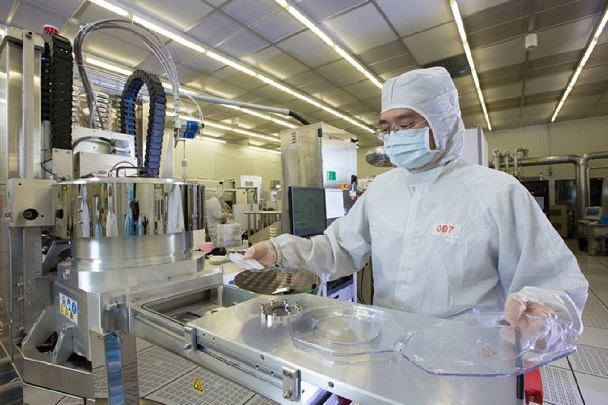
A semiconductor research centre in Taiwan (Representative Image)
When the Government of India announced its policy and incentives with an initial overlay of nearly $10 billion to develop a display and semiconductor ecosystem in India, there were four types(categories) of schemes. Display fabs, Semiconductor chip design and Silicon fabs are three of them.
The fourth scheme (notification from 21 Dec 2021 is available here) offered incentives for “Compound Semiconductors / Silicon Photonics (SiPh) / Sensors (including MEMS) Fab in India for manufacturing High Frequency / High Power / Optoelectronics devices”.
Perhaps due to administrative reasons (for example the percentage of incentive offered, similarity in the amount of investment needed etc), the policy and incentives for Semiconductor packaging, otherwise known as Assembly, Testing, Marking and Packaging (ATMP) or Outsourced Semiconductor Assembly and Testing (OSAT) was also combined into this “fourth category”.
Though not meant to be a comprehensive study, here is a quick look at various types of compound semiconductor fabs differentiating them from Silicon fabs.
Divisions within Semiconductor market
The semiconductor market is normally split into two major categories:
Integrated Circuits (ICs or more popularly “chips”)
Optoelectronics, Sensors and Discretes (OSD)
Market study groups differ slightly in their estimate of how much was the exact sales in these two categories. As per ICInsights, the total market in 2021 was over $600 billion of which ICs alone was over $500 billion and OSDs over $100 billion.
Despite inflation, soaring energy costs, ongoing glitches in supply chains, recent Covid-19 virus lockdowns in China, and Russia’s war with Ukraine, IC Insights continues to anticipate an 11 per cent increase in total semiconductor sales this year. As a medium and long term outlook, this overall semiconductor market is expected to reach $1 trillion by 2030-31 and $2 trillion by 2035-36.
A lot of products that will be made in “Compound Semiconductors / Silicon Photonics (SiPh) / Sensors (including MEMS) fabs" fall mostly under the “OSD'' category. The sensor part is obvious, the SiPh fabs and some compound semiconductor fabs make optoelectronics devices.
It is not necessary that fabs for Silicon Photonics and MEMS are always exclusive - many fabs that make Silicon based ICs also have facilities to do MEMS and SiPh. A lot of what “compound semiconductor fabs'' produce may fall under OSD and in some cases under “ICs”.
ICs can be further classified in various ways - for example digital-analog-mixed signal or memory-logic, whether general purpose or specific, reprogrammable or not etc. Most of those ICs continue to be made on Silicon - almost all microprocessors, memory and most analog chips for example. The conclusion part of this article has some thoughts on integrating compound semiconductors with Silicon for certain ICs.
What are compound semiconductors and their use?
There will be some element symbols used, so the reader may want to keep a periodic table handy.
Quoting from an article - "A compound semiconductor is a single-crystal semiconductor material composed of two or more different elements. Some of the widely used compound semiconductors include GaN, AlN, InSb, and GaAs from the III–V element groups and CdS, ZnSe, and HgTe from the II–VI groups… The article also summarizes the main challenge -Compared with silicon semiconductors, compound semiconductors are far more expensive and much more difficult to produce."
Then why use it ? "...compound semiconductor substrates that include silicon carbide (SiC), gallium arsenic(GaAs), gallium phosphorus(GaP) and gallium nitride are being used for LEDs. III-V compound semiconductor devices have an ability to function at higher frequencies, and the exploding demand in commercial broadband/wireless communication and optical communication technologies has led to wide application of compound semiconductor process technology in high frequency, high power, low noise, and optoelectronic products."
For those interested in the reasons for this, Table 1 in this paper compares important semiconductor parameters for Si, GaAs, SiC, and GaN which demonstrates the incentive of using GaAs (a direct gap semiconductor with high electron mobility) for high speed and optoelectronic devices, SiC (with its excellent thermal conductivity) for high power devices, and GaN for high power devices and optoelectronic devices for the ultraviolet range of frequencies.
Some of these points - especially high power, high frequency are mentioned in Government of India’s notification - "Rapidly increasing use of compound semiconductors in power semiconductors, radio frequency devices and LED applications is expected to drive the demand for the compound semiconductors... Compound Semiconductors provide faster switching at high power with increased energy efficiency and suitable for high temperature applications."
The notification asks for 150/200mm (wafer size) fabs in the compound semiconductor category while for Silicon fabs it has to be 300mm. Growing single crystalline Silicon wafers to bigger sizes is well established and the 300mm wafers have been around for two decades.
For compound semiconductors, the wafer is made using epitaxial growth and these have not yet scaled like the Silicon ones. In fact 100mm wafer fabs are still very common, sometimes 150mm while newer ones tend to be using 200mm. The capacity ask in the notification is 500 or more Wafer Starts / Month (in 100 mm equivalent) for compound semiconductor fabs compared to 40,000 or more 300mm wafers for Silicon fab - that itself will give an idea of the “smaller scale”
Note that using compound semiconducting material in a fab need not necessarily make it a “compound semiconductor fab”. For example, Germanium - used in the first transistor - is compatible with Silicon which makes it an easy add-on. Silicon Germanium (SiGe) technology can be processed using the same toolsets for Silicon wafers and is typically used for high performance. SiGe is also used for enhanced mobility in pFET for advanced nodes.
Also, SiC and GaN are “wide band gap” (WBG) materials- this article compares them with Silicon.
The wide band gap material does have some advantages in certain industries - for example automotive. Due to similarities in properties (for example the band gap), there is 'competition' between SiC and GaN itself in certain areas - here is an article with multiple examples and comparison. Notice that the word "device" is used many times and not "IC" or chip.
Global examples and India’s efforts
Presenting the details of each and every compound semiconductor and their application is beyond the scope of this article, however links to some interesting reads are below:
This presentation from Sandia National Laboratories will give many examples of where GaAs, InP and their combinations can be used.
This article covers GaAs specifically including R&D in India and global industry.
Here is an article on GaN and SiC and some challenges faced.
India is implementing “Gallium Nitride (GaN) Ecosystem Enabling Centre and Incubator for High Power and High Frequency Electronics” at IISc for Rs 300 crore.
Though one cannot vouch for the authenticity, a random search for reports with numbers for compound semiconductor market showed the following:
This one said that it is expected to grow from $32.0 billion in 2020 to $43.4 billion by 2025, a second one said its value surpassed $36.13 billion in 2021 and is expected to hit over $60.07 billion by 2030 and a third one said it is valued at $29.25 billion in 2019 and is projected to reach $47.13 billion by 2027 - about 6 per cent of overall semiconductor market.
Also here is an interview with numbers and names of industry players in the wide band gap material market.
As of 19 February 2022, as per this announcement there was only one applicant in the Compound Semiconductors / Silicon Photonics (SiPh) / Sensors category and that was for a SiC fab (detailed interview here). The deadline to apply in this category is 1 January 2025 and it is likely that more applications have already come by or will come soon.
Though the exact claims are debatable, China is said to be investing a lot in compound semiconductors. India’s push to achieve higher presence in this segment is applaudable however there should be a clear understanding that these are no substitute or match to Silicon fabs and that knowhow in one does not translate automatically to knowhow in the other.
Introducing ElectionsHQ + 50 Ground Reports Project
The 2024 elections might seem easy to guess, but there are some important questions that shouldn't be missed.
Do freebies still sway voters? Do people prioritise infrastructure when voting? How will Punjab vote?
The answers to these questions provide great insights into where we, as a country, are headed in the years to come.
Swarajya is starting a project with an aim to do 50 solid ground stories and a smart commentary service on WhatsApp, a one-of-a-kind. We'd love your support during this election season.
Click below to contribute.
Latest