Commentary
Mission Semiconductor: Can India Target 3 To 4% Of $1 Trillion Industry By 2030?
Arun Mampazhy
Mar 15, 2022, 08:09 AM | Updated 08:09 AM IST
Save & read from anywhere!
Bookmark stories for easy access on any device or the Swarajya app.


The recently-introduced European Chips Act aims to enable the European Union to realise its ambition of increasing its current market share of 9% in the overall global semiconductor industry to 20% by 2030.
On 15th Dec 2021, the government of India had announced a new incentive scheme worth Rs.76,000 crore INR (nearly $10.2 billion) in a bid to boost the semiconductor ecosystem in the country. In February, the government announced the details of the companies and consortiums that have applied for incentives, and in some cases, the quantum of total investment planned and the total incentives sought from the government.
Unlike in Europe, there is no target percentage or number for semiconductor fabrication (production) listed in any official policy documents or roadmaps released so far by the India semiconductor mission or any of the ministries under the government of India.
This article attempts to arrive at the quantifiable goal that India can seek to achieve.
While the semiconductor industry would predominantly mean integrated circuits (ICs or popularly known as chips), there are also related areas like Optoelectronics, Sensors and Discrete (together termed as "OSD").
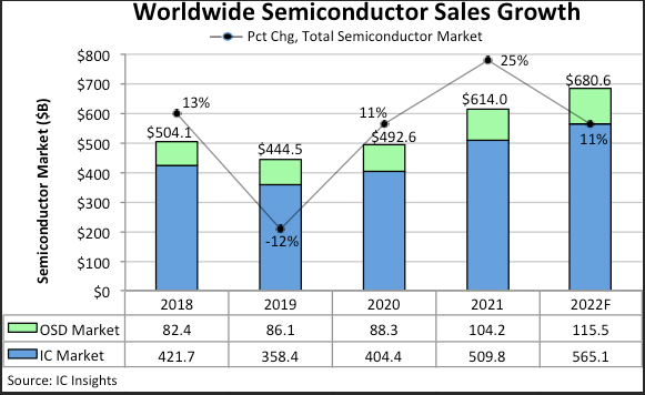
Market research firms estimate the revenue of the semiconductor industry using their own methodology. For example, in January 2022, ICinsights estimated that the IC market itself crossed $500 billion in 2021, and OSD crossed $100 billion. Gartner estimates 2021 semiconductor revenue at $583.5 billion.
In February this year, the Semiconductor Industry Association (SIA) announced that the global semiconductor industry sales totaled $555.9 billion in 2021. While numbers may diverge, everyone agrees that the semiconductor industry did cross the $500 billion mark at least (counting from the time of Intel's 4004, it took 50 years to get there.)

Predictions for the future vary, one of the optimistic ones coming from the CEO of Mubadala (the primary shareholder of GlobalFoundries)
"It is going to take probably eight to 10 years to double [$1 trillion or more by 2030 ~ 2031]. And it is going to double right after that, probably in four to five years[$2 trillion by 2035-36]," the CEO of Mubadala estimates
He is not the only one - the CEO of Applied Materials, one of the leading suppliers of equipment and other elements of the supply chain for semiconductor fabs, had also said "As an industry, we have line of sight to $1 trillion market in the next decade."
Foundry Revenues
Now let us look at the foundry revenue ( including contract chip fabrication. This category includes the contribution from pure-play foundries like TSMC, UMC, GlobalFoundries etc., and the foundry business of Integrated Device Manufacturers(IDMs) like Samsung, which makes chips for other companies in addition to making its own.
By October 2021, Trendforce predicted that foundry revenue would exceed $100 billion by October 2021. ICinsights had a prediction of $107.2 which is likely to be close to actual numbers in 2021 - a number complex to calculate accurately as companies like Samsung don't report the foundry revenue separately, leaving it to the analysts to guesstimate
If we compare the semiconductor sales revenue with the foundry-based revenue, the latter has been at a percentage close to 20% so far. However, one may see the later increase in the coming years as the advanced node chip fabrication is mainly restricted to a pure-play foundry (TSMC) or an IDM with a strong foundry business (Samsung). Intel, which is widely expected to catch up on advanced nodes, too, has jumped into contract chip manufacturing by announcing the setting up of a new vertical called Intel Foundry Services.
With overall annual semiconductor revenue likely to be somewhere around $1 trillion in 2030, the foundry revenue could be above $225 billion, probably even $300 billion. Given this revenue outlook, the question we examine here is how much of this can be "done on Indian soil" given the push by the government of India?
The phrase "on Indian soil" is used purposely because depending on whether a global chip manufacturer wholly owns the fabs that come up in India or operate through a joint venture with an Indian business partner or fully owned by an Indian group (who can license the technology from an MNC in a technology transfer arrangement), the market share that we aim to estimate may vary.
Similarly, how much of the chips fabricated in India will be used for domestic consumption vs exports will also depend on the fab loading models of the approved companies (Prime Minister Narendra Modi's vision of Make in India includes making for the world). The total revenue from the chips fabricated by "foundries on India soil" may be a good benchmark and also perhaps slightly easier to guess with some assumptions as below.
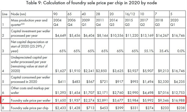
I will use the following table from this article as the basis for some of my calculations, mainly focusing on item #7, the estimated sale price of a processed wafer for various process nodes for TSMC. These numbers are indicative only as the actual price a foundry will be charging its customer may depend on many factors, including the complexity of the specific chip(s), how much volume they are ordering, the urgency, whether any special features are included and so on.

Now let us look at the Indian context. Out of the Silicon fab proposals received for the $10.2 billion incentive scheme, ISMC, with Tower semiconductors as a technology partner, is believed to have proposed a 65nm fab for $3 billion project cost. When the fab is fully up and running, capacity is expected to be 40,000 wafer starts per month (WSPM).
Suppose this project is approved soon and can reach full production by or a few years before 2030, and with further assumptions, the sale price will be slightly lesser than that of TSMC. In that case, there may be a mix of 65nm, 90nm and 130nm and the fab loading, yield and sales are of the order of 90% or more, a back of the envelope calculation will show that the annual revenue could be of the order of $600-$700 million.
Foxconn-Vedanta's proposal is said to be of a 28nm fab for a project cost of around $7.4 billion - it is not clear yet if Foxconn indeed has the knowhow or license or experience of running such a fab or if they will require further partnerships - these are for the experts at "India Semiconductor Mission" to evaluate.
This article focuses on the capacity and revenue estimate assuming the project approval and ramp-up to production and capacity. In this case, we assume a capacity of 40000 WSPM by 2030, and with assumptions similar to the previous case, the revenue generated could be of the order of $900-$1100 million
There are hardly any details of the third proposal by IGSS that I could find. Instead, I will refer to few pointers that emerged from what Union Minister For Electronics and Information Technology Ashwini Vaishnaw said in his interview to Swarajyamag that I was fortunate to anchor.
The Minister (at around 50:12) said that by 2030 India hopes to have at least four good silicon fabs and 40-50 compound semiconductor units. At around 43:00, he was asked if we would see TSMC or Samsung or Intel apply for a fab in India in future, he said an emphatic "Yes".
Let us assume that once the first set of fab(s) are approved, and they take off, more applications come and that at least one of that - either as a new applicant or as an addendum to the already approved ones - is that of a process node closer to or less than 20 nm. Depending on when such development happens, it could be running in partial or complete capacity by 2030. There is also the possibility of the approved ones increasing their capacity, say to 60,000 or even 80,000 WSPM
The compound semiconductor or similar smaller units could also generate income equivalent to a few 10s of millions of dollars, and there are also schemes for discrete component manufacturing. If all goes well and we add all these, a $2.5 billion annual foundry revenue being generated on Indian soil may be an achievable goal - that will be 1% of the assumed global revenue which was done earlier in this article.
Can we reach 2%? or a target of $5 billion? It depends on how fast the approvals are given for proposals received, the construction, ramp up, and fab loading happens and how quickly and of what type, capacity, and process nodes the future proposals may be for.
Achieving the first 1% will be crucial, and thereupon, it may grow faster like what happened with automotive manufacturing in India. As per this paper which quoted OICA data "India's ranking among automobile producing countries increased from 16th to 6th between 1999 and 2017, and its share in global passenger car production (in terms of number of cars) increased from 1.3% to 5%"
We zoomed in to the foundry revenue from the bigger umbrella of semiconductor revenue. With an assumption of 1-2% foundry revenue in India by 2030, can we now zoom out and hope for a 1-2% share of the expected $1 trillion semiconductor revenue? Well, that will depend on how the rest of the elements like Assembly, Testing and Packaging, fabless etc come up and also whether the fabs in India will all follow the foundry (contract manufacturing for others) model or will we also see some "Integrated Device Manufacturer" models - in other words, how much of successful product-based companies of scale will be there in India by 2030
Nearly three months after establishing "India Semiconductor Mission" (ISM), there is no confirmation yet of a team with a strong semiconductor and fab background leading it - Minister had hinted in the interview that there will be some news in a few weeks and that in the interim there are people working day and night in reviewing the applications received.
Let us hope that in addition to making sure that the execution of the project progresses at a good pace, the ISM leadership is also able to come up with an estimate of what India can target by 2030 in a much clearer and better way than this guesstimate that I have done.
Arun Mampazhy has a BTech from IITM and MS from University of Maryland in semiconductor fabrication and over a decade of industry experience. His dreams of seeing a commercial fab takeoff in India has changed from black and white to colour over two decades. He can be reached via email nanoarun(at)gmail(dot)com or @nano_arun on twitter. Views expressed are personal.


