Technology
DLI For Semiconductors: Should India's Chip Design Scheme Chase Innovation Or Numbers?
Ankit Saxena
Feb 25, 2025, 05:08 PM | Updated Apr 02, 2025, 02:42 PM IST
Save & read from anywhere!
Bookmark stories for easy access on any device or the Swarajya app.

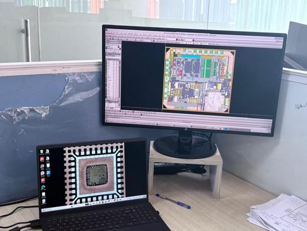
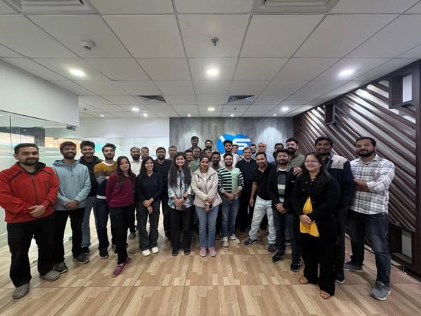
At a facility in Greater Noida’s Special Economic Zone (SEZ), a team is hard at work to craft an India-designed chip for a Korean company that manufactures weighing machines.
The team is from Vervesemi Microelectronics, a fabless semiconductor company specialising in analog signal chains and signal processing. (Fabless companies design but do not manufacture their own chips.)
The company ventured into this niche space at a time when semiconductor development in India received little to no attention.
“After having worked with ST Microelectronics since 1991 — a European multinational semiconductor design and contract manufacturing company — we started this venture in 2017 with the goal of doing something meaningful, and doing it in India," Rakesh Malik, the chief executive officer (CEO) of Vervesemi, tells Swarajya.
"Our initial designs include six patented innovations, covering applications in weighing scales, energy metering, sensor products, energy exploration, data acquisition SoCs, and thermal sensors. These designs are being utilised by multiple design companies," he adds.
In recent years, with India's recognition of the strategic importance of semiconductors and a focus on establishing a domestic ecosystem, the company has grown to become a significant player in this industry.
Vervesemi Microelectronics was the first company to be awarded incentives under the Centre's design-linked incentive (DLI) scheme.
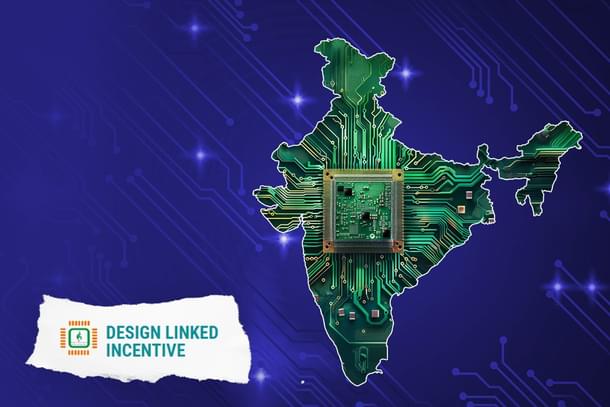
The DLI Scheme
Launched in December 2021, the DLI scheme aims to provide financial support and infrastructure assistance across various phases of semiconductor design, development, and deployment. It is a key component of the Union government's $10 billion semiconductor initiative spanning five years.
Currently, the scheme is available to domestic startups, offering financial support for semiconductor designs like integrated circuits (ICs), chipsets, system-on-chips (SoCs), and intellectual property (IP) cores intended for integration into electronic products.
Similar to the production-linked incentive (PLI) scheme — launched by the Indian government to boost domestic manufacturing through financial incentives tied to production targets — the DLI scheme focuses on semiconductor design and development within India.
The aim is to support a domestic semiconductor design ecosystem, reducing reliance on imported technologies.
With the introduction of DLI, every segment of the semiconductor and electronics supply chain — from components and sub-assemblies to finished goods — now benefits from subsidies.
The scheme focuses on:
Chip design infrastructure support, providing the advanced design infrastructure, including electronic design automation (EDA) tools, IP cores, multi-project wafer (MPW) fabrication support, and post-silicon validation access for approved companies
Product design-linked incentive (PDLI), where approved applicants engaged in semiconductor design can receive fiscal support covering up to 50 per cent of eligible expenditures, capped at Rs 15 crore per application
Deployment-linked incentive for companies whose semiconductor designs — ICs, chipsets, SoCs, systems, and semiconductor-linked IP cores — are deployed in electronic products. They receive an incentive of 6 per cent to 4 per cent of net sales turnover over five years, capped at Rs 30 crore per application
How Design Shapes the Semiconductor Landscape
Semiconductor development relies on a complex ecosystem involving multiple corporations.
In brief, "fabless" companies design chips, foundries (fabs) manufacture them, and OSAT (outsourced semiconductor assembly and test) facilities handle packaging and testing.
Chip design remains the first step, including circuit creation and assembly planning, carried out by fabless firms.
The second step, manufacturing, is handled by fabs. The Taiwan Semiconductor Manufacturing Company (TSMC) leads the global market, controlling over 50 per cent of production.
“These three — fabless, fabs, and OSAT — work independently but must coordinate. The design must match the fab’s technical nodes, and OSAT relies on the fab for final chip assembly,” says Dr Mukul Sarkar, Associate Professor at the Indian Institute of Technology (IIT), Delhi, and co-founder of 3rdiTech.
Incubated at IIT Delhi, 3rdiTech, a DLI-awarded Indian startup, specialises in defence chip designs. “Chip design is the foundation of the semiconductor industry, shaping how a chip performs before it is built. Fabless companies are at the forefront of innovation in the development process.”
“They are also the primary customers of foundries," he adds, "and while fabless firms grow quickly, fabs have a slower growth rate due to the high setup costs.”
India is reportedly home to nearly 20 per cent of the world’s semiconductor design engineers, who design around 3,000 chips annually. However, most of the work is for multinational companies (MNCs), limiting domestic IP creation.
Despite its talent pool, India lacks homegrown product companies, as most global firms retain product ownership and key IP at their headquarters.
“Almost all chips are imported. For instance, weighing scales rely on cards and chips from China and other Asian countries,” says Pratap Singh, chief technology officer (CTO) of Vervesemi Microelectronics. “Thus, supporting the design of these chips in India directly promotes import substitution, which is a key goal of the DLI scheme.”
"The fabless design process alone accounts for 50 per cent of the total semiconductor cost, with fabrication at 20-30 per cent and packaging around 10 per cent," he says.
"By promoting design, creating IPs, and increasing import substitution, India is addressing the largest cost component domestically.”
Support Through DLI
The DLI scheme aims to push Indian companies by helping them develop and own their products. It has made it easier for startups to take risks and innovate by reducing barriers.
Now that the first phase of the scheme is complete, its impact on homegrown companies can be guaged.
Applications were invited from January 2022 to December 2024.
“When we started, only two or three companies existed, some of which were later acquired by bigger players,” says Rakesh Malik, CEO of Vervesemi. Today, Vervesemi has grown into a team of 45 engineers with its own testing and technical support setup.
Most fabless companies begin at a small scale but can grow to thousands of employees, like Qualcomm or STMicroelectronics.
In India, however, production-based design firms currently operate at smaller scale. “The required tools and silicon are expensive, making entry into the industry difficult,” Malik adds. “But the DLI scheme is changing that.”
In 2023, Vervesemi received approval to design IP for motor control, applicable across multiple industries.
The first set of approvals included three companies. “The scheme is well thought-out. With one project underway, we are now preparing designs for two more, targeting energy exploration and space technology,” he says.
Most Indian companies have focused on outsourced services rather than product design, acting as support manpower for larger corporations.
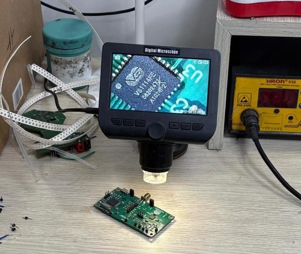
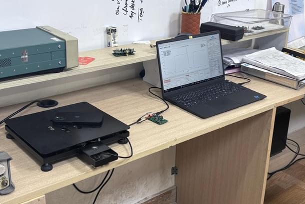
Chip development involves designing, testing through MPW runs — where multiple designs are tested together to share costs — and refining the design before moving to full-scale production.
The final step, MASK production, is extremely expensive, costing crores. It is, therefore, a significant barrier for smaller firms.
Without financial support, the industry lacked a strong incentive to innovate.
Lowering Entry Barriers
For fabless companies, major expenses include manpower, overhead costs, design tools, and raw materials for in-house testing, with design tools being the biggest financial burden.
The DLI scheme has eased this entry barrier by funding access to EDA tools, separate from the incentives provided for chip design, testing, and production.
The ChipIN Centre at the Centre for Development of Advanced Computing (C-DAC, the nodal agency) has been established as a centralised hub for chip design and fabrication services, supporting domestic startups and academia.
Over 100 institutions nationwide are already leveraging this infrastructure under the C2S programme, using tools from Cadence, Synopsys, Siemens EDA, Ansys, and Xilinx.
Through the national EDA grid, startups selected for the DLI programme can use advanced design tools, enhancing their product development capabilities.
“This access serves as a stepping stone for emerging companies, enabling them to develop feasible proposals aligned with the scheme’s vision,” Pratap tells Swarajya.
Limited Approvals Have Raised Concerns
So far, 17 companies across Delhi NCR (National Capital Region), Karnataka, Telangana, Kerala, and Tamil Nadu have been approved under the financial support (PDLI) scheme.
These include:
Vervesemi Microelectronics (Greater Noida) – Microcontroller ICs for industrial applications
DV2JS Innovation (3rditech) – Image sensor SoCs for automotive applications
Fermionic Design (Bengaluru) – Beamformer ICs for satellite communication
Morphing Machines (Bengaluru) – RISC-V multi-core accelerators for telecom applications
Calligo Technologies (Bengaluru) – Hardware accelerators for AI
Sensesemi Technologies (Bengaluru) – Wearable SoCs for healthcare applications
Saankhya Labs (Bengaluru) – Base station SoCs for 5G communication
Aheesa Digital Innovations (Chennai) – Networking SoCs for telecom applications
Netrasemi (Thiruvananthapuram) – Edge-AI SoCs for smart vision and IoT applications
Green PMU Semi (Hyderabad) – Energy-harvesting power management ICs for IoT and sensing applications
WiSig Networks (Hyderabad) – NarrowBand IoT SoCs
MosChip Technologies (Hyderabad) – Smart energy meter ICs
Over 50 companies have been approved for EDA tool support, enabling them to develop and refine products to meet the financial assistance criteria under the DLI scheme.
The government initially set a goal of funding at least 100 startups over five years, targeting 20 approvals per year. However, actual approvals have fallen short of this goal.
Further, as per updates from September 2024, the total estimated cost of these approved projects is Rs 342 crore, with the government committing around Rs 133 crore.
The Ministry of Electronics and Information Technology (MeitY) maintains that these incentives will be reserved for Indian companies. Requests from MNCs are not being accepted currently.
Explaining the approval process, Pratap said, “The process involves financial scrutiny, multiple levels of technical evaluation, and an assessment of the commercial viability of the proposed product. Special emphasis is placed on the Indian market and its potential for import substitution.”
“The focus is on quality over quantity. Seventeen approvals mean 17 different product designs. How is that a bad thing? The methodology is sound, and both the nodal agency and MeitY are handling it exceptionally well,” he added.
But not everyone shares this viewpoint.
Varied Views On Scheme's Implementation
Many have raised issues concerning implementation.
First, early-stage startups believe the evaluation process should be more structured and efficient, avoiding unnecessary repetitions and focusing on the right questions at the initial stages.
Shashank Jha, CEO of Reslink, tells Swarajya, "There are many new-age companies with highly talented engineers, but India’s semiconductor ecosystem is still in its early stages. Unlike other industries with established legacy firms, this sector is just beginning to take shape. The current evaluation process should align with the stage we are at, and the criteria should be reasonable for startups."
"The process should be strict, challenging, and demanding — but it must also be relevant to the current stage of the industry. The DLI scheme is a great initiative to build this ecosystem, but there is a need for some rethinking in its implementation," he adds.
A policy expert argues that the strict due diligence process at an early stage is hindering the growth of domestic startups. Many of these companies struggle to prove their commercial viability, meet data sheet requirements, and fulfill broader industry criteria.
If evaluation process becomes just about fulfilling paperwork requirements to secure incentives, it could divert companies from the core goal of innovation and domestic product development.
A similar situation occurred with the PLI scheme, where manufacturing remained limited to assembly, merely meeting government criteria rather than bringing true value addition.
Second, since most companies are still at a very early stage, the current incentive structure does not create a level playing field.
The semiconductor industry is capital-intensive, making it difficult for many startups to progress beyond initial tool access.
Experts suggest that initial financial and tool support should be extended to all applicants, with a review process after a year to determine which companies should continue receiving assistance.
"Many early-stage companies benefiting from EDA tool support struggle to move beyond the design phase. The 50 per cent incentive is helpful, but when considering the overall project costs, such as manpower and operational expenses, it becomes difficult for companies to even begin," says an industry expert.
They emphasise that the process should remain strict, focusing on quality and innovation. However, given the current position of most Indian semiconductor startups, revisiting the implementation strategy and ensuring stronger initial support is crucial for long-term success.
Third, with this progress, various agencies have suggested modifications to help the initiative gain more momentum.
As per reports, the India Cellular and Electronics Association (ICEA) suggested that the scheme should allow MNCs to participate, provided they design chips within India.
However, many startups believe that allowing MNCs could dilute the scheme’s core objective — supporting homegrown semiconductor companies to sustain in the long run.
“Ten years ago, there were barely any such startups in India, but now, with government support, the numbers are growing. For any semiconductor ecosystem to thrive, strong government backing is essential,” Dr Sarkar says.
He further points out that major global semiconductor players emerged through long-term government policies and incentives.
"With that in place, the success metric should not be the number of companies selected under the scheme within a given timeframe. Instead, the focus should be on the quality of innovations, policy support, and on future expansion,” he adds.
Feedback to Shape DLI 2.0
According to Dr Sarkar, it is also time to consider the next steps. First, strategies to reduce the commercial burden once the subsidies under the scheme come to an end.
Reaching self-sufficiency in this industry is not a short-term goal. India's ambition to achieve Aatmanirbharta (self-reliance) and become a key player in the global semiconductor value chain requires long-term financial support.
"The impact of this initiative will only become evident after four to five years. If these companies are left to survive on their own once subsidies end, many will struggle."
"Ultimately, economics will drive technological growth, not the other way around," he adds. "We need a well-structured long-term strategy beyond fixed subsidy periods to ensure these companies can sustain themselves and focus on innovation."
Second, the current state of affairs highlights the importance of niche designs for the country and reduce direct competition with global players. “For example, Vervesemi is working on chips for space technology. Similarly, defence applications currently rely on imported chips from South Korea and China. Developing indigenous intellectual property in such niche areas will strengthen the domestic ecosystem."
However, the rush for numbers may shift focus away from niche design towards generic chip development.
Startups working with widely known IPs will face intense competition from established global fabless companies once their products reach the market.
Third, while looking at the larger semiconductor ecosystem, India must also start working on coordination between chip designers, fabs, and OSAT facilities.
Currently, India is setting up fab and OSAT facilities in Gujarat and Assam, but without coordination with the domestic chip design industry, these facilities will have to rely only on foreign customers to operate at full capacity.
At present, globally, semiconductor fabs are concentrated in Taiwan, South Korea, the United States (US), and China. Most India-designed chips are also tested and produced at these facilities.
Thus, as India builds its own infrastructure, early planning, such as for technological node alignment and collaborations, remains crucial.
Get Swarajya in your inbox.
Magazine