Technology
Fab In India: A Case For Pure-Play Foundry To Foster Indian Fabless Ecosystem
Dr Santhosh Onkar And Dr Veeresh Deshpande
Jan 11, 2021, 03:15 PM | Updated Jan 12, 2021, 03:44 PM IST
Save & read from anywhere!
Bookmark stories for easy access on any device or the Swarajya app.


Every US dollar the US federal government invested in semiconductor industry/research increased the overall U.S. gross domestic product (GDP) by $16.50.
This impact of semiconductor technology is due its pervasive role in many sectors like automotive, agriculture, bio-medical, defence, space, industrial automation etc.
Indian vision for a 5 USD trillion economy will remain far-fetched, if this strategic investment is procrastinated further. Semiconductor technology is the essential brick needed to build the infrastructure of secure, self-reliant ‘digital India’.
This article is an exploration of the avenues with low-entry barrier to jump-start Indian semiconductor industry.
Industry body ASSOCHAM data shows that “Under normal operation of the industry, India imports about USD 5 billion worth electronic goods”. In 2020, this demand is expected to have crossed USD 400 billion (CAGR of 41 per cent).
The Indian Semiconductor design (i.e. Fabless) market is projected to surpass USD 52 billion (CAGR of 29 per cent).
Hence the Government of India has a strong incentive to catalyse the formation of a Pure-Play foundry in India.

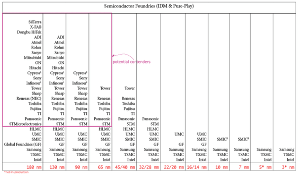
Moore’s law (Intel’s co-founder Gordon Moore in 1975 made an observation that number of transistors that could fit on a chip would double every 2 years) has knocked-out all but three major players competing at the bleeding edge nodes (10 nm or less) of silicon transistor manufacturing.
One of the primary reasons for it is that advanced transistor technology (<45 nm nodes) is very costly, requiring significant investment in research and development as well as in production to achieve reasonable yield.
Only a strong customer base (requiring millions of chipsets) can sustain these technologies. The demand for these advanced transistor nodes is primarily driven by the processor designs of major players like Apple, NVIDIA, and Qualcomm whose major products are high-speed, low-power digital processors (generally CPUs or GPUs) for mobile devices, PCs or data servers.
However, there are many companies catering to other applications of semiconductor chips not necessarily using advanced nodes, and instead, the comparatively low-cost nodes.
Entry point for Pure-Play Foundry in India
A large number of chips are still made using 180nm, 130nm or 90 nm technology, especially analog mixed-signal and radio frequency chips (RF) used in phones and wireless devices, devices for the Internet of Things (IoT), industrial and automotive applications.
Since it is a mature technology, acquiring the manufacturing equipment is likely to be cheaper at a fully depreciated price point, and therefore, the process can be quite attractive from a cost standpoint.
This is where FabinIndia needs to hedge its bets with realistic chances of taking-off and pursue it relentlessly on mission mode unlike aimless duds of the yesteryears.
A second part of this article will explore technical aspects of such a fab and its potential advantages for the Indian economy.
A local fab has benefits like the obvious fillip to the efforts towards a “manufacturing economy” to begin with. Further, it will provide meaningful extension to the Government of India’s “Design in India” initiative, graduating to the actual “Make in India” for semiconductor chips.
From the business perspective, this provides a vital additional pure-play foundry option to many start-ups or fabless design houses in India and shorten their time-to-market.
Additionally, this has the potential for spin-offs encouraging entrepreneurial engineers languishing inside big semiconductor design centres in India or abroad.
The downstream benefit of this will be the emergence of the “assembly and system integration” ecosystem. The capacity building for manufacturing precision multi-layered printed circuit boards (PCBs) at a competitive price point is the disruption needed to become “Atmannirbhar” and create products for actual local needs.
The assembling, packaging and testing infrastructure will propel the dormant semiconductor enterprise to transform from a predominantly service industry to manufacturing.
A pure-play foundry at low-entry technology nodes will help iron-out the initial woes of supply chains, tooling, machinery setup and yield-centric device engineering expertise.
It will prepare the ground for established foundries to set-up offshore fabrication units to maintain their older nodes at low cost and also load-sharing for any unplanned demand surge like in 2020, which is expected increase further in 2021.
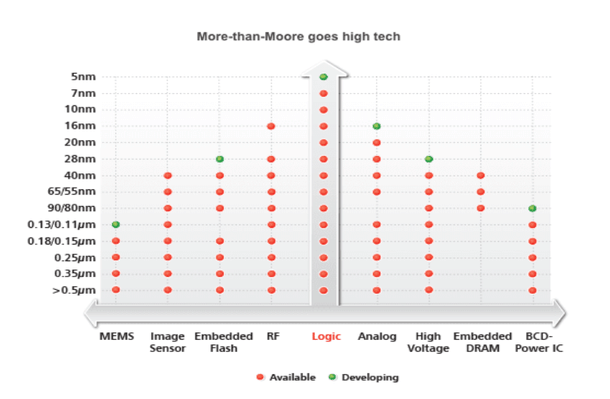
More-than-Moore (2.5D/3D packaging & MEMS) and RISC-V
Even though the big three (Intel, Samsung and TSMC) may continue to churn silicon wafers in bleeding edge nodes at 3nm based on their road-maps at least for next decade, the technological limits to the progression of Moore’s law have nudged the industry to explore exotic technology options.
2.5D and 3D packaging options are an interesting blend of high-speed digital silicon from advanced nodes like 10 nm or below cohabiting with high-precise analogue realised in much larger node (65nm or 45nm) on a die-to-die bonding, nano-packaging or PCB.
It is a route worth exploring if FabinIndia becomes a reality.
Further, Micro-Electro-Mechanical systems (MEMS) combined with the Analog data acquisition is the common denominator, be it healthcare industry or gig economy of Industry 4.0 and if played well, India might still get a portion of the Industry 4.0 market.
There are many derived or second-order benefits of the semiconductor industry learning with significant impact in other industries. For example, microfluidic chips for DNA sequencing machines, essential for studying the epidemiology of SARS-CoV-2, is something that can be fabricated in older technology nodes.
RISC-V open architecture, a relatively unexplored (only in tiny island research centres in India) could be scaled-up and re-purposed to many industry and academic needs if they can be fabricated in India.

Metallisation of the weak academic and industry interconnect
Barring a handful of engineers at premier institutes, who manage to get a peek at fabricated silicon thanks to their collaboration with industry, Indian academia churns out engineers (especially Electronics and Communication or VLSI post-graduates), who have never had the luxury of taping out a VLSI design or testing a silicon chip.
Most of these electronics graduates end up as coding engineers just like the graduates from other engineering disciplines.
The training institutes mushroomed in Bengaluru or Hyderabad serve the industry demand for EDA trained engineers, but still without any exposure to an actual silicon.
A fab house running Multi-Project-Wafers (MPWs) like BRAHMA (hypothetical) accumulating designs from pan-India universities along the line of MOSIS (in US) or EUROPRACTICE (in EU) would do wonders to ignite design innovations in India.
Even though the Pure-Play Foundry is a capital-intensive industry to set up, it has a strategic imperative for India on multiple fronts like defence, space and more importantly, it will bolster fabless ecosystems to grow and thrive.
India will be on the familiar path of the semiconductor fab industry inceptions pursued by US, Taiwan, Germany, France, Israel and China who have all incentivised (30 per cent or more of the total costs) the semiconductor industry.
Indian Inception Parallels — Pharma and Space Indigenisation
Finally, a brief look in the rear-view mirror to find inspiration parallels in Indian drive on path to industrialisation. The Chemical Industrial and Pharmaceutical Laboratories Ltd. (known as Cipla since 1984) was set up in 1935 by Khwaja Abdul Hamied.
It took 17 years (1952) for it to realise the need for self-sufficiency in technological development — only to be materialised by Yusuf K Hamied (Yuku) — son of K.A. Hamied returning to India after his Ph.D at Cambridge.
Yuku’s ordeals with red tape in the initial years are tales for another day. A brief mention that regulations of a public traded company needed government’s approval a) to hire anyone related to a company director and b) to set that appointee’s salary, which meant Yuku worked initially for free (almost US$20 for subsequent 3 years).
Ranjit and Gurbax launched Ranbaxy (combining their first names) with a modest goal of distributing foreign drugs in India in 1937.
Today, as the world battles with a raging pandemic, Indian pharma is standing shoulder-to-shoulder with the world in devising and supplying a viable vaccine to the entire world starting with India.
The Indian Space industry (although in its early stage) also has an equally popular founding legend. Starting with Vikram Sarabhai’s role in the formation of the Indian National Committee for Space Research (INCOSPAR) in 1962 and the Indian Space Research Organisation (ISRO) in 1969, the recent successes of Mars orbiter have catapulted India for greater aspiration in space technologies.
Indian Space industry spin-off from ISRO Labs is a promising model to emulate for the Indian semiconductor industry. The government should consider an industry-focussed and partnered semiconductor research and development lab that will funnel needed innovations for semiconductor manufacturing in India.
A similar model has been successfully implemented in other countries. For example, ITRI (in Taiwan) or IMEC & CEA-LETI (in EU). It can bolster the Indian semiconductor manufacturing ecosystem (to be explored further in the subject of an upcoming article).
In summary, (excuse the cliché): “Semiconductor Fab in India is an idea whose time had come, gone and has returned (due to pandemic), but only with a narrow window of opportunity before it is gone again for the foreseeable future.”
(This is Part-1 in a series on the semiconductor industry in India.)


