Economy
#FabInIndia: Why Creating Demand For Chips Is Key To Boosting Semiconductor Manufacturing
- The question is what the government can do to ensure that it is the chips produced in the country that will be used in products like mobiles or laptops sold in India or exported out of the country.
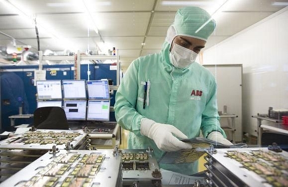
A semiconductor plant in India.
Today (2 July) marks one month of the announcement of three schemes by the government of India through the Ministry of Electronics and Information Technology (MEITY) to boost electronic manufacturing in the country as part of its ambitious Atma Nirbhar Bharat Abhiyan.
From what I know, PLI scheme is getting good traction, but there is no news yet of any semiconductor chip (IC) manufacturers going for the incentives offered in Scheme for Promotion of Manufacturing of Electronic Components and Semiconductors (SPECS) and Electronics Manufacturing Clusters-2 (EMC2) schemes.
My article titled "India's big push" analysing these schemes from the perspective of their usefulness towards realising semiconductor chip (IC) manufacturing units (fabs or foundries) was published by Swarajya on 5 June.
After the martyrdom of Indian soldiers at the hands of the Chinese, I wrote two more articles in Swarajya, out of which, this article explained why India need not go for cutting edge <28nm technology nodes to begin with.
There will be enough market till 2025 and beyond for products from an analog fab with technologies in the 45/65nm to 130/180nm range and a digital fab with say a 28nm and an additional 45nm capability.
An approximate estimate of the investment needed for those two fabs with around 20,000-30,000 processed wafers (that is, wafers each on which multiple chips are fabricated) per month capacity each will be around $1.5 billion and $2.5 billion respectively.
It will also be good if these are part of a cluster of fabs — let us say in addition to these, there is also an R&D fab, a testing facility and a niche III-V fab. A III-V fab, instead of silicon wafers as starting material, uses wafers made out of materials like GaN or InAs or combinations of multiple elements from the III and V groups of the periodic table.
Chips made from III-V wafers could be of much importance in space applications as they work in extreme low-temperatures and also for some high-end power and defence parts or equipment.
My suggested cluster of five fabs is not just coming out of the EMC2 scheme's clause of "CFCs must cater to at least five units to get 75 per cent incentive" logic, but also from the need for such ecosystems manufacturing a wide range of chips and components that go as inputs into ATMP units.
I wonder what happened to the Rs 2,500 crore "GaN fab" that was proposed two years ago. An initial reading indicates that the end product proposed was "wafers" and not "chips" — wafer is only the starting material for chips, but that is good too to begin with.
I will be glad to stand corrected that there were also plans to make chips or small components using those wafers, whether it is within the Rs 2,500 crore or not. In fact, I hope that there will be follow up article soon about where that attempt is.
Note that the estimates I gave so far for silicon based analog and digital fabs assume that silicon wafers will be bought, which is what many fabs do.
Setting up silicon wafer making plants will need additional investment and could be considered in India once the wafer-to-chip fabs are in place. I will continue to use the word "fab" to mainly mean wafer-to-chip manufacturing units, especially in the context of silicon-based ones.
Each of these fabs could be opened by different foundry players, and each of these could have different investors — in fact, even one big-shot Indian investor or a few getting into the semiconductor fab business will give the much needed boost and confidence to the top foundry players like TSMC or Samsung or GlobalFoundries or UMC or Towerjazz to come set up units in India.
SMIC being Chinese, is better to be avoided. I must also say that we need not wait for investors or players needed for all five fabs, if someone is ready to invest in one, let us say the silicon based analog fab or the III-V and get going, the others will follow — and the differentiation on technology and purpose ensures collaboration than competition among the five.
One month may be too less a time to assess whether SPECS has even reached the doorstep of any big foundry player or investor, leave aside them expressing interest.
However, given that both US (through its "The American Foundries Act of 2020") and China (through its "Made in China 2025" initiative) have decided to go big in the semiconductor fab space and a $119 billion master plan from Samsung already is on the roll in South Korea. Government of India has to take quick decisions.
The "next wave" of foundries have already begun, much of it directly driven by the governments like is the case with the US and China. India need not go for the top of the wave, but can India at least get some momentum?
Let Us Now Examine What Would Be Some Of The Quick Decisions Needed Towards That
In my 25 June article requesting India's Prime Minister for "3Ds" — to "declare intent", "dedicate a body or a technocrat" and to "develop FPIs to reach Indian investors and eventually FDIs" , there is also a "tailpiece", quoting an article on whether yet another scheme or policy may be in the making to trigger #FabInIndia — perhaps a "25 per cent before production" plus "25 per cent once production starts" (both of which could be grants or reimbursements that need not be returned to the government) plus a 25 per cent interest free loan.
Until I see such a scheme really come out, I continue to view it as speculation. I see no point in the government waiting to finalise it, or if it is not in the making to deny it categorically. Time is of essence in the semiconductor race. If SPECS is the "Hobson's choice", so be it, but say so loud and clear.
A few days back, I had the opportunity to listen at length to Mr "MA" (don’t read too much into the choice of the initials, they are just the initials of my name reversed, to keep the identity of the person low profile for now).
Mr MA is part of an attempt to realise #FabInIndia. I asked him, "are you ready to press the button if the government announces an even bigger incentive than what is offered in SPECS, let us say the 25 per cent + 25 per cent + 25 per cent incentive scheme?"
His reply was calm but firm "Arun, imagine I have $1 billion. Let us say, I also get $1 billion + $1 billion + $1 billion through government schemes and use the $4 billion for two fabs with the help of one or two global foundry players.
In two to three years when the fabs are ready to ramp up production, how do I ensure that demand for chips will feed my fabs and make sure that the line is running full? If I don't get that assurance, I may just want to put that $ 1 billion as perpetual fixed deposits, even my future generations can live out of the interest earned."
Mind you, he is not saying without having done a market study — his group apparently has already done a thorough analysis which showed that out of the 78 electronic products used in India, 25 dominate with 95 per cent both in terms of volume and value, and they have analysed the technology roadmaps of the chips that go into it.
The conclusions on the "which tech-nodes-to-go-for" match with what I independently presented on 18 June in Swarajya. So the question is not whether the chips produced using those technologies have a market in general.
It is more about what India can do, to ensure that it is the chips produced in India, or by those foundries who have committed to help with #FabInIndia that will be used in products like mobiles or laptops or others that are sold in India or exported out of India.
In short, Mr MA's ask for the government is a preferential market access (PMA) policy for semiconductor chips (ICs) — perhaps it is already there for PSUs, now the request to the government is to implement it for key private sector segments too.
The "pull" strategy through PMA could be a substitute or an addendum to the "push" schemes like SPECS and is something that the government should seriously consider, especially in a situation if the push schemes still do not trigger #FabInIndia.
I am no expert at this, but let me extrapolate and give an example — perhaps not quite the example that Mr MA is trying — as far as I know, this is not the foundry player that he is in touch with. Let us look at the smartphone market shares in India from first quarter of 2020 and compare with the numbers from various quarters of 2019.
Clearly, Samsung is losing out to others — I will leave it to the readers to figure out "How much Chinese" some of the others in the list are. Now imagine if there is a policy which can lead to a situation where if Samsung signs an MoU to help set up #FabInIndia, there will be some incentives.
A tough decision which may have immediate consequences, but which can help India in the long term and in its pursuit to excel. Adding another perspective, how long will India satiate its young electronics engineers with service jobs?
Another example is the case of Huawei, this time in a "non-preferred" way. On 30 June, WION news published this, which said, "When Huawei was given the green light to participate in the 5G trials in India, the company breathed a sigh of relief. Huawei may have dodged a bullet then. But now, it faces fire and perhaps a global ban".
A few hours later there was also the news from the US — "The Federal Communication Commission has declared Chinese telecom giants Huawei and ZTE “national security threats,” a move that will formally ban US telecom companies from using federal funds to buy and install Huawei and ZTE equipment".
In December 2019, Observer Research Foundation had published a detailed analysis titled "5G Infrastructure, Huawei’s Techno-Economic Advantages and India’s National Security Concerns".
India must strongly look into the case and also look at who benefits if Huawei is "non-preferred" or banned, and parallelly India Inc can check which fabs produce the chips that will eventually go into the players that could get an upper hand with such a move and try to bring those fabs to India through collaboration.
Semiconductor fab is one area where solid actions demonstrating the "India Inc will rise to the occasion" comment will help and it will be beneficial to the core business owned by many of them as well. Given that not only will there be a huge need for chips — especially coming out of analog fab — for handsets and base stations needed in 5G, the future differentiation of many other products including automotive and other machinery also may be driven by the quantity and quality of electronics in them.
However, the government of India may need to create environments conducive for India Inc and take steps to assure that they will get good return on investments.
Back to Mr MA, who by the way did not give me these examples, but only the idea of having PMAs for semiconductor chips in India. I further asked him — "Won’t it take two to three years for a fab to come up and make chips in India? How can the government of India implement a PMA for semiconductor chips when there is none making them in India?"
His answer was "virtual fab". Hoping that my understanding of what he explained is not "lost in translation", the idea seems to be, sign MoUs that binds one or more foundry players with a commitment to open fabs in India, and starting right away and till the physical fab comes up in India, route the chips via an Indian subsidiary.
If that Indian subsidiary is part of or the driver for eventually realising the physical fabs in India, it is even better. I will leave it at this and hope experts take the debate forward.
Interestingly, former ambassador G Parthasarathy has been quite vocal for #FabInIndia as per this video, and though he perhaps doesn't say PMA , he seems to be asking for Indian collaboration with TSMC.
I have pointed out in my 18 June article that TSMC is not the only Taiwan-based player, there is UMC too, and there are also South Korea, UAE and Israel based players in the list of top six.
It will be great if one of the top two — TSMC or Samsung — finds India as a possible landing space for some of their older tech-node efforts or experimental technology efforts but with both of them too focused on the <10nm race, India should also look at the others in the list.
Fifteen years ago when there were attempts at #FabInIndia, there were some who said, "Oh, it is too difficult for us to do it" or even "We don't need them".
Now, many say, "India should have done it 15 years back". Let us not have the next-generation say "India should have done something at least in 2020".
This year, 5 July is Gurupoornima. The thought of #FabInIndia was "etched" into my brain first by my BTech project guide at IIT Madras — Dr K N Bhat — during a casual conversation sometime in the year 2000 or 2001. Many more teachers, colleagues and friends have helped shape my thoughts and given valuable inputs. As Gurupoornima nears, I would humbly like to state that if I ever wrote anything correct or useful, it is thanks to my gurus. Mistakes or flawed logic if any are purely mine.
Support Swarajya's 50 Ground Reports Project & Sponsor A Story
Every general election Swarajya does a 50 ground reports project.
Aimed only at serious readers and those who appreciate the nuances of political undercurrents, the project provides a sense of India's electoral landscape. As you know, these reports are produced after considerable investment of travel, time and effort on the ground.
This time too we've kicked off the project in style and have covered over 30 constituencies already. If you're someone who appreciates such work and have enjoyed our coverage please consider sponsoring a ground report for just Rs 2999 to Rs 19,999 - it goes a long way in helping us produce more quality reportage.
You can also back this project by becoming a subscriber for as little as Rs 999 - so do click on this links and choose a plan that suits you and back us.
Click below to contribute.
Latest