Technology
Some Strategic, Defence And Data Security Reasons For #FabInIndia And Possible Options Before GoI Post EoI Deadline
- To give some context to the "strategic" importance of semiconductor fabs, some information from a private-public model adopted for decades in the US and some recent US-based studies are being presented below.
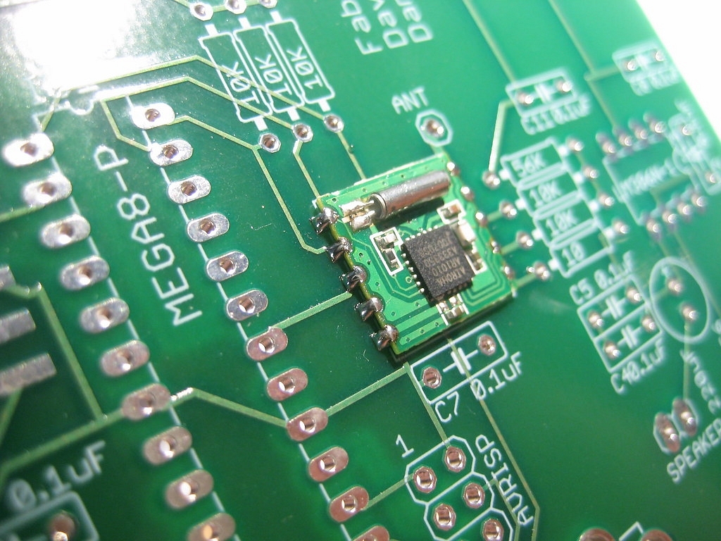
A chipset.
While the US continues to aggressively push for "on-shoring" more and more of the semiconductor chip manufacturing, the Government of India has to expedite taking its baby steps.
MEITY's 15-Dec-2020 Expression of Interest (EoI) for semiconductor fabs (foundry) seems to have received some attention in the media as well as from potentially interested parties.
How many of the interested groups will indeed submit good proposals by the deadline (as of now 31-Jan-2021) is to be seen — indications are that there may be one or a few private groups.
MEITY plans to decide on the incentive schemes based on the proposals it gets.
An Economic Times (ET) article gives an overview of what the government may be hoping to see happen. Meanwhile another report in ET on 28 December 2020 mentioned that ISRO is planning to build an additional fab under the Semiconductor Lab (SCL) that it currently owns.
Being more like a news item, one cannot expect technical details and accuracy in such a report, and ISRO or SCL may not want to reveal much about future plans either, including whether they are eyeing an expansion to cater to strategic needs only, or is there a plan to turn SCL into a potential fab for commercial chip (IC) needs too.
To give some context to the "strategic" importance of semiconductor fabs, some information from a private-public model adopted for decades in the US and some recent US-based studies are being presented below.
Trusted Foundry Program: Details can be read here, in a nutshell — “The program provides a cost-effective means to assure the integrity and confidentiality of integrated circuits during design and manufacturing while providing the US Government with access to leading edge microelectronics technologies for both Trusted and non-sensitive applications”.
In a common man’s language, the US government strikes a deal with a private firm to fabricate the chips and there are stringent restrictions on who can view or review the design (IP), work in the fab etc — it has to be certified US citizens, while physically present in the US.
This arrangement is said to have been first made with IBM sometime in the 90s (since GlobalFoundries bought IBM fabs in 2015, now the US facility of the latter is a Trusted Foundry too) and extended to other companies in 2007 or so.
Recently, some "review" and churn of this model is ongoing in US as below
A “TAME” (Trusted and Assured Micro-Electronics) report that came out in December 2019 and available here . It talks about “multiple CPU hardware vulnerabilities – Meltdown, Spectre, Foreshadow, and even a new variant of Rowhammer to name a few” , and also that "vulnerabilities in the IPs and Trojans inserted in the manufacturing process (hardware design, fabrication, packaging, etc.) have turned into a growing concern. Worse, since most semiconductor companies are focusing on design only and becoming “fab-less”, malicious hardware modifications and Trojans can be inserted at fabrication time by untrusted foundries".
It is not clear whether this report played any part in a new thought process at the US Department of Defense — captured to a good extent in this May 2020 article wherein it said "...the department looks instead to a "zero trust" approach to purchasing microelectronics. That assumes that nothing the department buys is safe, and that everything must be validated before it can be used."
Note that the new proposed approach too does not indicate any US government plans to directly own fabs.
Even in an article published on 15 January 2021 about the US measures, it seems more about localisation of facilities and creating "tiers of trust".
"There should also be public-private partnerships to share risks and accelerate availability. And partnerships with allies are required to ensure uninterrupted, secure supply chains..... " .. "Considering security of production and the supply chain, physical location may provide a level of inherent trust or assurance. "
"Initiatives like the CHIPS for America Act and the American Foundries Act must support world class domestic commercial technology. They must balance cost, quality and a secure supply chain, to extend domestic advantage and secure the electronics supply chain as critical infrastructure".
An article in IEEE spectrum hints that the thrust may be more on giving incentives to attract more private investments.
"The SIA calculates that a $20-billion incentive program over 10 years would yield 14 new fabs and attract $174 billion in investment versus 9 fabs and $69 billion without the federal incentives. A $50-billion program would yield 19 fabs and attract $279 billion".
Note though that there are "non-Silicon-based" fabrication facilities owned by the US Department of Defence directly or through collaboration with US Universities and other organisations where cutting edge advanced material (like compound semiconductor) based chips can be fabricated in limited volume which are likely used in space (which needs many chips to work at extreme low temperature for which III-V based chips are typically used) and some highly critical security applications.
The Trusted foundry model and the new “zero trust” approach may be much more relevant for Silicon based fabs - where the same article previously quoted says "Today... commercial demand dominates the market by a large margin, with defense electronics being less than 1 percent, but remaining essential to national security".
Make-in-India efforts in defence and allied areas cannot ignore these important studies and must look at the need for IC fabs in India — more exclusive facilities to cater to strategic needs and/or Trusted Foundry model hoping that commercial #FabInIndia will at some point become a reality, early indications of which may be known after the current EoI deadline.
So then, is expanding SCL to be able to cater to commercial needs an option? Like it or not, in such a case, "track record" becomes somewhat important and one naturally would expect some clarity on the following points about its "current status".
1) Is the current mass production capability of SCL at best 180nm technology on 200mm wafer size?
There is a line in the ET article that talks about 65nm “capacity”. To the best of my knowledge, there is no mass production (stepper and photomask based) capability for SCL in 65nm.
If they meant being able to develop a prototype chip using e-beam writing, that by no means qualifies as mass production — same holds for the line about SITAR having a “100nm capability”.
2) The 2019-2020 budget summary of SCL available here says nearly 370 crore rupees on Operations and 270 crore rupees on Capital — are there any details on how they were spent ?
Likewise, any sense of how much of “Returns” was there on the money spent?
3) What is the capacity in Wafer Starts Per Month (WSPM) for the current facility at Mohali?
How much of that is currently utilised on an average?
On the third point above, hearsay is that SCL’s current capacity (WSPM) is miniscule compared to usual commercial fabs, and that itself is under utilized — not at all a good situation if it were in a commercial fab. Commercial fabs need to be near fully-utilized, running near 24x7x365 to be profitable.
From some cursory searches on the internet, it appears that after a design is submitted, to make the photomask, SCL has to issue tenders, and if that is indeed the case, that kind of wait time will not be liked by any chip design company (client) — will be glad to be corrected if any of these pieces of information are incorrect.
Given that so far SCL may have been used only for some academic and very limited strategic chip needs, such information and discussions about capacity, efficiency, profitability and so on may not have mattered much. However, if SCL wants to get into catering to commercial IC needs taking public or private funding, these are extremely important matters to be looked into.
ISRO comes under the Prime Minister himself, so either there maybe a plan for PMO to directly fund the SCL expansion plans, or SCL/ISRO will have to submit an EoI through MEITY.
After the EoI deadline, we may come to know if and what SCL has opted for — and the capacity that it has requested for will give us an idea whether SCL is indeed eyeing a commercial fab.
If it is the latter (whether it comes through MEITY EoI or directly from PMO), the big questions will be how much of solid study and preparation would SCL have done and what plans it has to be run like a business as opposed to a "typical Indian PSU".
If it is 65nm tech-node mass production capability that SCL desires to expand into, that may be driven mainly by the NAVIC kind of chips, which falls under the larger RF-Analog domain and that is an area where it is confirmed that there is a recent crunch of chip availability — quoting from this 21 December 2020 extremetech article, it is now felt that not enough investment was done globally in Analog/RF centric fabs and that “A great many IoT and 5G chips are built on 200mm, as are some analog processors, MEMS devices, and RF solutions” .
Those points and a detailed analysis is what was written in this August 2020 article titled — 5G, IoT And More: What Chips Can $1.2 Billion To $2 Billion ‘Analog’ #FabInIndia Make?
To put it in short, India urgently — i.e. within the next 1-2 years — needs to have a good commercial fab that can 'mass produce' (at least 20,000 WSPM 300mm equivalent) analog centric chips, with additional mixed signal capability.
Starting with such a 130nm/65nm fab and perhaps adding a 28nm digital fab also within 2-3 years would be a good start. In other words, these are the tech-nodes and kind of fabs that are likely to be proposed (if any) by private groups too in an effort to start commercial #FabInIndia and it will be interesting to see if SCL will also eye for them.
One can continue to 'dream' that a TSMC takes interest in a 5nm of 3nm fab facility in India or someone takes interest in atleast a 14nm or 16nm, but unless they have solid plans on multiple fronts — investors, technology partners and market — it may yet again end up as all talk and no take-off
To summarise, by 31 January 2021, if there are no private players with a proposal for a commercial fab based on EoI for either the 28nm or below digital or a 130nm/65nm mixed-signal/analog fab, then the option left for Government of India may be to look into expanding SCL's capabilities to satisfy strategic needs and perhaps even some part of Make-in-India commercial needs.
Maximum efforts that may be possible for a PSU to try for profitability and ensuring efficiency should be attempted.
However, if there are proposals from private groups for commercial #FabInIndia that are convincing enough (clear road map on Investments other than government incentives, Technology partners with good track record etc) for one or both or more of those tech-nodes or types, then they should definitely be supported with maximum incentives possible because in addition to giving a major boost to Atma Nirbhar Bharat in the commercial I/C space, it will also give Government of India a chance to explore a Trusted Foundry or similar model, further boosting Make-in-India for defence and strategic applications.
Academics and electronic industry startups in India could look at MOSIS kind of arrangements through "MPW"s, explained in this June-2020 ORF article and also in this 11 January 2021 article — the latter details how #FabInIndia will be good for fabless-in-India too.
In the latter scenario, a limited capacity expansion of SCL for extra-strategic chip needs can be an additional option for India.
Support Swarajya's 50 Ground Reports Project & Sponsor A Story
Every general election Swarajya does a 50 ground reports project.
Aimed only at serious readers and those who appreciate the nuances of political undercurrents, the project provides a sense of India's electoral landscape. As you know, these reports are produced after considerable investment of travel, time and effort on the ground.
This time too we've kicked off the project in style and have covered over 30 constituencies already. If you're someone who appreciates such work and have enjoyed our coverage please consider sponsoring a ground report for just Rs 2999 to Rs 19,999 - it goes a long way in helping us produce more quality reportage.
You can also back this project by becoming a subscriber for as little as Rs 999 - so do click on this links and choose a plan that suits you and back us.
Click below to contribute.
Latest