Tech
Many Upcoming IC Fabs Do Not Need EUV or >$3 Billion Investment, Contrary To What Some May Think
Arun Mampazhy
Jul 05, 2021, 04:49 PM | Updated 04:49 PM IST
Save & read from anywhere!
Bookmark stories for easy access on any device or the Swarajya app.


The famous physicist Richard Feynman in this video talks about the difference between knowing the name of something and the knowledge of that something.
In many discussions about semiconductor IC fabs, it has increasingly become a fashion for many to throw around words like EUV, and investment costs of anywhere between $8b to $15b for fabs that use "EUV".
Some even use that as an excuse to discourage India from having a commercial semiconductor fab.
Unfortunately, more often than not, when asked about details, the same people are clueless of the "why and where" EUV is needed — we will settle that in the second half of this article.
The first half of this article will give some examples of how what was written more than a year ago in the context of what kind of commercial semiconductor fabs can India aim to have as a beginning, is now being vindicated by many global examples.
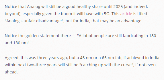
The relevant quote is as follows:

In fact, the current global chip shortage, which started making into Indian mainstream media around February or March 2021, started with chips that are made using mature nodes — which some unfortunately think are outdated.
For example, here is news from December 2020 and note that the fabs that process wafers of size 200mm typically have technology nodes upwards of 90nm — for example 130nm, 180nm, 250nm, 350nm, 500nm and so on.
Fabs that processes 300mm size wafers typically do 90nm and below, while they can also do the three-digit nanometer nodes if there is demand and the necessary technology qualifications are done.
And now here are a list — by no means exhaustive — of most recent developments globally that vindicates the stand that for India, a 45nm or 65nm (and hence processing 300mm size wafers) Analog or Analog and Mixed Signal fab is in no means outdated, but instead, a good start.
1) On 23 June 2021, media reported GlobalFoundries (now fourth in terms of foundry revenue, after TSMC, Samsung and UMC) CEO as stating:
The industry has painted itself into a corner by focusing on single-digit nanometer....Today we have cars sitting in a parking lot missing chips made on 45 or 65 nanometer
In the news, also notice that the amount estimated to raise the capacity in Singapore (where it already has multiple fabs) is $4billion and there is also a mention of one of the close rivals United Microelectronics Corp (UMC) planning $2.8 billion investment for a new fab.
2) ST Microelectronics and Israel's Tower Semi are collaborating to build a 300mm wafer processing fab in Italy and the press note says:
In the early stage 130, 90 and 65nm processes for smart power, analog mixed signal and RF processes will be qualified in R3. The products in these technologies will be notably used in automotive, industrial and personal electronics applications
Note that as early as December 2019, an Indo-Israel study had proposed a similar fab for India and $0.9 billion subsidy and $1.1 billion interest free loan were sought to make it happen.
Though it was never officially mentioned anywhere, one can make an educated guess on which is likely to be the fab from Israel which led this study.
3) Texas Instruments recently bought a fab from Micron and here is what it said: "The company is currently planning to equip the fab for the production of analog and embedded processors on the 65nm and 45nm nodes."
4) Bosch recently inaugurated a new fab which makes chips using 65nm technology, processing 300mm wafers and the investment cost is $1.2 billion. Part of the reason why the cost is low could be that Bosch already has the technology (and so the cost of tech-transfer from another fab is not there) and perhaps the capacity is not so big.
For India, since a commercial fab — if and when it happens — will be a first, a bit more will be needed for 300mm fabs — for example for a 65nm fab anywhere between 2-3$B depending on capacity (measured in wafer starts per month or WSPM), whether there are plans to use refurbished equipment, how costly is the tech-transfer and so on.
A new commercial 200mm fab can perhaps be achieved for the 1.2$B, but then, return on investment will have to be studied, given that 300mm wafer holds nearly 2.25 times the number of chips (of the same size) that a 200mm wafer can hold and also the scope of growth beyond this decade may be limited.
In fact, as this article was being written, there is news of a Chinese company buying a UK based 200mm fab which, going by their website, has 180-700nm technology and 32,000 WSPM capacity, expandable to 44,000 — and what is interesting is that the deal is reportedly for just $87 million!
It is sad that Indian firms are either not even aware of such possibilities or are not interested, despite the possibility of the government giving incentives even for such outside India buyout, as per "Category C" of the expression of interest here.
If not anything, it could have been at least an opportunity for Indian firms to "get their hands dirty" and perhaps even transfer some of that knowledge and more to India eventually.
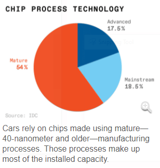
A recent analysis in IEEE spectrum mentions that 10 new 200mm fabs being setup, and getting equipments for 200mm fabs have become tougher — had India attempted this 5-6 years back, it may have been a success now, especially given the kind of statistics presented in the below picture from the same IEEE analysis.

It may not yet be too late and for those interested in knowing what has been happening on the prospects of a commercial #FabInIndia, they can look up the series of articles here, the latest ones have information on where it stands, the only somewhat significant news seen after that is of the India Electronics and Semiconductor Association (IESA) Chairman being quoted in the media as saying:
Over 20 semiconductor manufacturing and designing companies in high-end, display and specialty fabrication have submitted expressions of interest (EOIs) to set up manufacturing plants in India. Of this, two-three are ‘very serious’ projects
(Note: It is not clear what he means by 'specialty' fab; one can hope that it includes an Analog fab).
There are (existing) incentives which are already in place like $1 billion incentive per chip company wanting to set up their manufacturing unit in the country. The government is open to increase the incentive amount depending on the investment the company is bringing to the country. They wanted to mention a figure to create interest, but this also means that they are not restricting the figures to $100,000 or $1 million or a billion. As the government starts engaging with the companies participating, clarity on incentives will start becoming apparent.
(Note: To the best of this author's knowledge, there is no official confirmation of the $1 billion incentive. It's also very important that these incentives are finalised at the earliest).
Now, let us go back to the question of EUV. While this is not intended to be a full-fledged technical explanation, some background information will be useful for better understanding.
A high level process flow in the world of ICs can be — requirements, architecture, circuit level design, physical design, fabrication and testing.
Depending on which technology node and the complexity, the 'physical design' gets split into multiple "layers" for fabrication.
For example, the gate (for the transistor) will be one level, and the first metal is another, though note that for advanced nodes, it gets much more complicated and the total layers can run into more than 100. However, not all layers will have the same kind of 'critical dimension'. For example, the minimum feature size for the 10th metal layer may be in three-digit nanometer even for a sub-10nm technology node chip.
With a 193nm wavelength source, using additional techniques like immersion lithography, multiple patterning and so on, many foundries have made chips up to 10 nm node.
Even many chips at 7 nm node chips are still made with such tools.
EUV or Extreme UltraViolet indicates light of wavelength in the range 10nm to 120nm. Current lithography tools using EUV focus typically on the 11-14nm range and the most commonly used one is 13.5nm.
The increase in resolution is not the direct ratio of 193 and 13.5 because of other factors — details of which are beyond the scope here. However, 7nm becomes 'easier' with EUV and for 5nm, 3nm and so on EUV litho is the proven way for high volume production.
Litho tools using EUV have very many challenges — they are huge, need extreme high vacuum, uses big power, need multiple cooling systems, instead of lense systems for 193nm based litho tools. These need mirrors that are extremely extremely flat and by the way, the photomasks needed for every layer are no more the glass type as is the case up to the 193nm litho tool, but yet again the reflective type.
No wonder only one company (ASML) predominantly makes these 'monsters' and very few fabs (TSMC, Samsung and Intel for high volume production, though Intel of course is yet to get its 7nm into production, and a few like IBM for research and early development) use them.
So now, if a fab is doing 7nm or 5nm or 3nm chips, will all the layers go through EUV lithography?
No way; only a few layers which have the minimum feature size and shapes that are very difficult to do with 193 nm tools will need to go through EUV lithography; the rest will continue to go through 193nm tools or even earlier ones like 248nm based lithographic tools and so on.
In short, only those fabs that do 7nm or below really need EUV based litho tools.
Given that there are zero commercial fabs in India currently, we can't expect a company to straight away start a sub-10nm fab in India. We will need to take it slow and steady; 65nm would be a good start, tech-nodes somewhere in the 20s (i.e 20 or 22nm or 28nm) could be the next 'logical' ones to have.
If we start in 2021, this much itself may take up to 2025 to materialise and depending on how well they do and how the market and demand looks then and beyond, it can be assessed whether tech-nodes in the 10s (10nm or 14/16nm) or the ones needing EUV based litho tools will be practical for India.
Arun Mampazhy has a BTech from IITM and MS from University of Maryland in semiconductor fabrication and over a decade of industry experience. His dreams of seeing a commercial fab takeoff in India has changed from black and white to colour over two decades. He can be reached via email nanoarun(at)gmail(dot)com or @nano_arun on twitter. Views expressed are personal.


