Technology
As Chip Packaging Industry Shows Signs Of Taking Off In India, Here Is A Primer For Beginners
Swarajya Staff
Aug 05, 2022, 02:59 PM | Updated 02:59 PM IST
Save & read from anywhere!
Bookmark stories for easy access on any device or the Swarajya app.


In its quest to achieve a certain degree of self-sufficiency in semiconductor manufacturing, India is hoping to bring up both commercial chip fabrication industries (fabs) as well as chip packaging industries (OSAT/ATMP as explained later in this article).
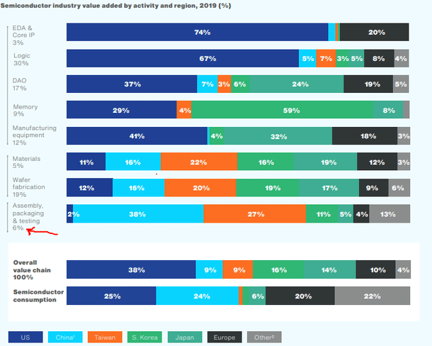
Even though of relatively lesser value add as shown below, lower investment and quicker to start advantages are helping the packaging units to take off sooner.

What happens to a "chip" before packaging? Multiple chip dies are "fabricated" through thousands of steps on each wafer in facilities known as fabs. Silicon wafers are the most common.
The size of the starting Silicon wafer predominantly used nowadays is 300mm in diameter and the one before this generation is 200mm in diameter.
The size of a die itself can be usually a maximum of around 26mm X 33mm and so multiple dies can be fabricated on each 300mm or 200mm wafer.
Within each die, there could be a single complex chip or multiple lesser complex chips. Historically each chip used to be diced out and packaged.
In Wafer Level Packaging techniques, the packaging is done on whole wafers and chips are diced only after the packaging is successfully completed.
What does chip packaging involve?
Here is a video that explains some basics of chip packaging:
Here is one more video that gives an idea of some more advanced types of packaging:
How are "OSAT" and "ATMP" different?
OSAT stands for Outsourced Semiconductor Assembly and Testing. ATMP stands for Assembly Testing Marking and Packaging.
In an exclusive interview given to Swarajya, Raja Manickam, CEO of Tata Electronics (OSAT) explained that "Loosely, we refer to OSAT as packaging and testing for multiple customers and ATMP is packaging and testing that is captive for a particular company".
India's incentives for ATMP units under "SPECS": Scheme for Promotion of Manufacturing of Electronic Components and Semiconductors (SPECS) was notified/launched in April/June 2020. The Scheme mentioned, "An incentive of 25 per cent on capital expenditure shall be provided to the units making investment for the goods as per list annexed. The incentive will be provided on reimbursement basis."
In the annexure, category C with a minimum investment threshold of Rs 25 crore includes ATMP.
The Scheme is open for applications initially for three years from the date of its notification. This could be the reason that the government does not seems to have released information on which companies have applied for under SPECS scheme, however there are at least two examples as below that Swarajya is aware.
In exclusive interviews given to Swarajya, Dr Harshad Mehta of Ruttonsha and Shiv Kumar of Sahasra Semiconductors had both confirmed to have applied for incentives under the SPECS scheme. Note that Ruttonsha's 200 crore plan falls under the compound semiconductor category - read how they are different from Silicon fabs.
For Ruttonsha, Phase1 plan is making Silicon Carbide wafers, Phase2 is to fabricate power electronic devices and Phase3 involves dicing the devices from the processed wafers and packaging them. After Phase1, Ruttonsha wants to focus on Phase3 and hopes to have that facility ready sometime between December 2022 and March 2023.
In July 2022, however, Dr Mehta sent a message stating: "We were approved, we began investing and completed Phase1 but now the government is creating all roadblocks for SPECS approval which we do need to raise funds to continue the implementation with phase 2 and 3. I am totally frustrated and disappointed".
Mr Shiv Kumar confirmed that Sahasra Semiconductors has obtained approval under the Production Linked Incentive (PLI), SPECS, and customised incentive from the state government for NAND Flash Memory packaging and testing and are on target to start manufacturing (packaging) by first quarter of 2023.
India's incentives for OSAT/ATMP under recent Semicon scheme: Under the Semicon incentives scheme launched on 15 December 2021 with Rs 76,000 crore overlay, incentive of up to 30 per cent on Capital expenditure for OSAT/ATMP is offered and the scheme is open till end of 2024. Detailed notification and guidelines can be found here.
By 19th February 2022, four companies were listed as having applied for OSAT/ATMP under the new scheme and some information is given in this report . By now, many more are said to have applied but the latest list is not available. Sahasra Semiconductors is also planning to apply for LED driver chip packaging.
Tata Electronics has not yet announced finalisation of its $300 million OSAT plans, according to a report in Economic Times in the month of May, they have surveyed four states - Tamil Nadu, Karnataka, Telangana and Odisha as prospective locations.
In recent news of what appears to be yet another investment in an OSAT/ATMP plant in India, a company named Polymatech claimed to have made a $130 million investment already. It claims to have received "in-principle approval" for 25 per cent subsidy on Capex and also says it has plans for $1 billion investment by 2025.
Good beginning, but what could be the challenges?
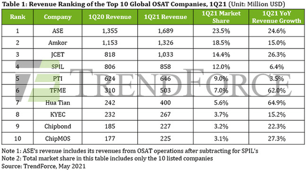
The not so complex OSAT facilities are already well established in many parts of the world and Indian units will have to compete with them.

For more advanced packaging, as this article notes, "In the race for heterogeneous integration, key players, such as ASE (w/SPIL & USI), TSMC, Intel, Amkor, and JCET, have announced unprecedented CapEx investment in 2021" . As an example, a recent news said that "Italy is close to clinching a deal initially worth $5 billion with Intel to build an advanced semiconductor packaging and assembly plant in the country."
In his interview, Raja Manickam noted that Advanced Packaging or Heterogenous Packaging is an inflection point and India has opportunities, however, there are challenges.
Shiv Kumar of Sahasra Semiconductors had highlighted the fact that since India still does not have commercial fabs, we do not have raw material (processed wafers) available domestically and it will not be available for the next at least eight to 10 years on a large scale.
Also Read: Rise (Part 1): Ramping Up India’s First Fab To Higher Capacity


