Technology
Facts, Fallacies And Future Of India's Efforts To Have Commercial Chip Fabs
- Here's where India's ambition to manufacture semiconductor chips at home stands as of October 2021.
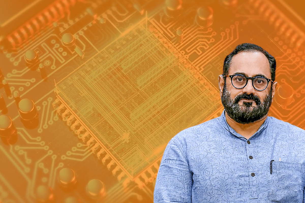
Minister of State for Electronics and IT Rajeev Chandrashekhar
When my first article in Swarajya was published on 5 June 2020 on the topic of why India needs to establish semiconductor fabs or chip (ICs) manufacturing foundries, few knew that there was a global chip shortage coming up by the end of 2020.
The first article did not mention any companies, and it was in my second article on 18 June 2020 that the now well known TSMC was mentioned, along with Samsung, Intel and others.
If you are a beginner on the topic, this brief video, albeit made about 16 months back, maybe of help, especially in understanding the wafer sizes (these days mostly 200mm and 300mm for Silicon-based chips) being processed, the technology nodes (like 350nm,250nm, ..., 90nm, 65nm, ..., 7nm, 5nm, ...) and so on.
Along my over a dozen articles in Swarajya on the topic, apart from brief mentions here and there, I did not focus much on the cliché lines that most journalists write on the topic, namely "Multiple attempts at establishing a commercial fab in India have failed in the past...". The other oft-repeated statement is that "IC fabs need lot of ultra pure water, uninterrupted electricity and many doubt that India can provide these". Some journalists also find Indian "experts" to then conclude that "It will never take off in India".
For someone who wants to see India succeed, there is no point in saying again and again that India has failed in the past unless you can bring out the lessons to be learned. Moreover, some reasons relevant at that time may not even be valid now. However, it appears that these oft-repeated negative statements, many times by Indians themselves, have created impressions and trust deficits which can only be repaired by actually making at least one fab take off in the near future - nothing succeeds like success.
So I delve into the past briefly - perhaps a regular reader of my articles may find some points repeated - with a note that as the story behind some of those are brought out, you may form your own opinions on lessons learned, and later as the attempts by the present government are presented, judge whether the necessary course correction is in place.
An effort started in around 2006 by a group called SemIndia with collaboration from Advanced Micro Devices (AMD) ran into investor or fundraising issues by 2008 compounded by the 2009 development of AMD going fabless - that is, AMD kept the design responsibility with itself and spun off a separate company named GlobalFoundries to do the "fabrication".
Going fabless also gave AMD the freedom to approach other such "pure play foundries" like TSMC for manufacturing. The 2007 'interest shown' by Intel did not materialise because the then UPA-1 government was too slow and missed the window (as per this Forbes report which quoted the then Intel Chairman).
In 2014, a few months before UPA 2.0 government stepped down, it issued Letters of Intent to two consortia for an overall Rs 63,000 crore investment plan and the official explanation of why both did not take off is mentioned in this article - in summary, an outgoing government may have taken a bit too high of an aim (for the India of those times), passed on the "burden of waiting for the consortia to come up with their part of the funding" to the Modi 1.0 government. One may also note that one of the technology partners involved, namely IBM, went fabless in 2015 (selling its fabs 'yet again' to GlobalFoundries)
The failure of a lesser known effort - a 2015 proposal by Cricket semiconductors for Rs 6,000 crore Analog fab, who wanted to break ground in 2016, but pulled out by early 2017 - is said to be because the government, this time Modi 1.0 was slow in its response (as per this report).
Cricket semi had most likely proposed a fab which can process 200mm size wafers, and in such fabs, the technology node used are 90nm and older (130, 180nm, etc.) - some had apparently discouraged the proposal terming it as "using outdated tech-nodes", but there was actually surge in demand for chips made in 200mm fabs in 2017-18 as well as in Dec-2020. Had the fab proposed by Cricket semi taken off in 2016, it is likely to have done well and/or at least the "India can't do it" barrier would have been breached.
Now with renewed global efforts in 2020-21 to resolve the chip crunch, the capacity equations are changing and it will be prudent to have Silicon fabs that can process 300mm wafers. 65nm or 45nm capable Analog centric fab of 20,000-40,000 wafer starts per month (WSPM) capacity and 20-28nm capable digital fabs (also of similar capacity) will be good for a start in India, and even the first one among those will be a good "stand up first before you try to walk or run" attempt for India.
While we are on the topic of technology nodes, a common misunderstanding even among some folks who work in allied fields is that all chips made these days are in technology nodes like 5nm, 7nm and so on need huge (of the order of $12 billion to $20 billion) investment per fab and that tools like ASML's EUV based step and scan systems are a must.
The fact is that a lot of chips are still made in two digit and some even in three digit tech-nodes - I have explained this in some detail as well as given examples and investment figures of many new fabs that are coming up globally with mature nodes, in this article.
On the infrastructure front, starting with electricity, I will present as an example, the number and method quoted for one of the earlier proposed fabs - one with 28nm technology node and 40,000 WSPM capacity - the pdf is available here, and the relevant portion reads as follows, of course, this is just one of the many methods and locations possible.
As for water, some calculations including the fact that a bigger amount is de-ionised and purified, are shown in this Twitter thread. Just for comparison, the Idukki dam in Kerala recently reached its red alert limit, and on 19 October, three shutters were opened to release excess water at the rate of 1 lakh litres per second. The daily water need for a fab that may need 10 million litres per day (MLD) can be fulfilled with the water coming out in less than 2 minutes.
These data points are presented not to trivialise the electricity and water requirements for fabs - they are not trivial - but they are very much doable in many parts of India. Reputed companies who set up and operate these infrastructure elements for fabs outside India have even assessed and okayed locations in India.
Let me now move from the initial section to the next section, that is, to the "Modi 2.0" era - a brief summary of some announcements by the present government during 2019-20 are presented in this article and more including an Expression of Interest (EoI) opened in December 2020 inviting proposals to establish #FabInIndia in this one.
Before we get into what happened (or did not happen) to the EoI, two news items that went somewhat viral this year related to this topic need a closer look.
News item 1: Multiple media reports a few months ago created an impression that Tata electronics has already decided to set up an IC (chip) #FabInIndia. No such decision has been taken or at least not officially announced. If you read this report carefully, it says "In the first phase, the Hosur facility will focus on hi-tech electronics manufacturing and is likely to plan semiconductor manufacturing in the next phase, a Tata Sons spokesperson said".
The "manufacturing" mentioned in the first phase is, in all likelihood "Outsourced Semiconductor Assembly and Test" (OSAT) and/or manufacturing of some non-electronic components that go into mobiles. There is no word yet on when the next phase of "semiconductor manufacturing" is planned and whether it is to make "discrete devices" or indeed Integrated Circuit (chip) fabs. I hope they will, that they will soon, and that the decision will include chip fabs.
News item 2: On 31 March 2021, Reuters reported that "The (Indian) government will give cash incentives of more than $1 billion to each company which will set up chip fabrication units" however the source was a "senior government official who declined to be named". A few days later, it was reiterated yet again through "other sources" (one wonders if this 'planted media reports' are done so that there is room for 'plausible deniability') - this report quoted IESA Chairman as saying:
“There are (existing) incentives which are already in place like $1 billion incentive per chip company wanting to set up their manufacturing unit in the country. The government is open to increase the incentive amount depending on the investment the company is bringing to the country."
Till date, there is no official confirmation of any such incentives, nor is there any decision taken about approving or rejecting the proposals received via the EoI, which was opened on 15 December 2020 and closed on 30 April 2021. Various news reports had reported that 15 to 20 proposals were received via the EoI and some of them are good - for the sake of India's reputation, the government should explain why the good proposals are still kept in suspended animation - even going by the closing date, it is already close to 6 months.
Some of the groups who put in the proposal are being asked if reimbursements will be okay instead of upfront incentives, and at times apparently, the discussions are being mixed up with "What can be done with SCL?".
Semi-Conductor Laboratory (SCL) in Mohali is an ISRO owned fab, which does 180nm technology node process on 200mm wafers in very low volume (something like 600 wafers per month when typically commercial fabs will have 20,000 to 30,000 wafers per month being processed).
Fabs being high Capex, can break even only if they do high volume production, and even if the government is considering to upgrade SCL to a 300mm fab with 65nm or 45nm technology, as long as it remains in government control, it is likely to not be able to run more than 1,000 or 2,000 wafers a month, which will be giving pathetic Return on Investments.
Even if each processed wafer fetches a profit margin of $1,000 (which is a number on the higher end), with a 2,000 WSPM capacity, you can get a maximum of $24 million a year - not even 1 per cent of a $2.5 billion or $3 billion investment needed, not to mention the operational cost.
20,000 WSPM would be the minimum capacity needed to have some hopes of break even, 30,000 or 40,000 will be a "safer" bet. Indeed, filling the capacity is a challenge, but for sure a commercial fab will be in a much better position to attract orders than a government-run one.
One may wonder, "But isn't necessary for security reasons that government owns a fab?".
First of all, it is doubtful that the process followed currently at SCL itself is any foolproof to data leakage (for example, between the design being received by the fab and the photomask for each level being made).
Secondly, it will be worthwhile for the government to study the Trusted Foundry model (a summary of which is presented in this article) followed by the US government for technology nodes up to 14nm and the new "RAMP-C" program for more advanced technology nodes as explained here.
In both cases, the emphasis is on the government supporting a commercial, private fab while also ensuring that it gets a secure and assured line of production. The US government recognises the fact that volume production is needed before the chips made using a particular technology node is mature enough, and for that, a commercial fab is a must.
Clearly, SCL has been a white elephant for the government and it may be only natural that the government is considering to privatise it, but mixing it up with fresh efforts at establishing private or PPP fabs in India is likely to be counterproductive. There are other options available for SCL -- given that it already has a 200mm production line and equipment suited for the same, it could be converted into a commercial compound semiconductor fab.
Globally many compound semi fabs are now transitioning from 150mm fabs to 200mm. Note that compound semi fabs can in no way be a substitute for Silicon fabs, they can be "additional" ones and have their own challenges.
One of the proposals put in via the EoI is by a group called Next Orbit Ventures with Israel based Tower semiconductors as its technology partner, a detailed interview of which is published here. Founder of the group Ajay Jalan in a later conversation mentioned that they already have land, water, electricity etc. and $360 million promised by the government of Gujarat and are looking for the $1 billion upfront cash to be finalised and approved from central government as was mentioned in the Reuters news - and with that, they can start work on the ground at the earliest.
However, in early September this year, Tower semi escalated by writing to Prime Minister Narendra Modi about the delay in taking a decision on a matter that is as time-critical as this. It is surprising - apart from the technological advantage that it can bring forth to India, it could also be a politically "useful" move for the PM given that Gujarat will go for state assembly elections by the end of next year and making this happen can be a good example for Modi's oft-made "double engine government" claim.
Meanwhile, in a report that came out in end-September, the new Minister of State for MEITY Rajeev Chandrashekhar was quoted as saying:
"As part of broadening and deepening our electronics manufacturing and electronics capabilities, we have a plan that was very quickly worked on after I joined the ministry on 7 July, and you will be seeing this being rolled out in October."
However, on 15 October, Vijayadashami day, in reply to a reminder tweet by this author, the Minister said the following in which there was no mention of manufacturing:
Other reports like this indicate that MEITY may soon open a "Request for Proposal" (RFP) inviting commercial bids, though it is not clear if the incentive structure will be part of the RFP or yet again the RFP will ask for "what kind of incentives are you looking for?". If it is the latter, it effectively means that after nearly a year, the government is back to square one - perhaps the new ministers at MEITY want a reboot of efforts, for reasons best known to them.
While there is no way that we can "make semiconductor chips in India by mid-2022" as it will be 3-5 years from approval to production, "The government is aiming to lay the foundation of the country’s first semiconductor manufacturing unit by June-July next year" as mentioned in the report is doable if only government does the right things quickly - in fact, it is already late and if the government had given enough priority to the matter right after the December 2020 EoI, the "foundation" could have happened by now itself.
Better late than never, but then there is no surety on whether this is yet another attempt by the government to hide behind (planted) rumours' in the media, buy time and come mid-2022, repeat, "You will see something happening in another six months". Rajeev Chandrashekhar's quote from the ET report also had this:
"We want to be capable providers, global leaders in the systems design part, and with some luck, semiconductor design. If the Prime Minister's vision really plays out, we will soon have a fab in this country in the next three to five years".
It appears that even ministers are waiting for some kind of approval from the Prime Minister before taking decisions on the incentives for fabs. Modi though, has made statements (paraphrased) like "Any technology anywhere in the world, India should have the capability in the upcoming decade", and the Financial Express report quotes Minister Ashwini Vaishnaw as saying "It’s the Prime Minister’s dream to have semiconductors designed and made in India", has so far not made a direct statement about #FabInIndia.
Also noteworthy is that both the ministers' quotes seem to say "a fab", "first fab" etc. - if what is planned is a policy with incentives finalised, shouldn't the government be expecting many players to come in?
Or is the government in itself deciding location, technology partner etc, for just one fab and putting it up only for investors? Even if such a plan exists, why limit it only to that, shouldn't it also take the already received proposals via EoI to a logical end, that too fairly quickly as they have been waiting for 6 to 10 months already?
Some say that Modi talks about something only after he or his minister does the groundwork and the news about "India and Taiwan are in talks to set up a $7.5 billion fab in India" as well as taking it up through quad are indications of these.
However, efforts via quad as of now seem at just a theoretical stage and there is also the big question of how much, how fast and at what cost the US or even Japan-based companies will transfer their manufacturing know-how, if at all.
Likewise, we can only hope that the government of India has considered all possible scenarios, including the "China attacking Taiwan within the next few years" scenario while trying to make a deal if what is reported in the media about such talks are true.
One can only hope that the attitude of "we will decide only if a big name and big money is involved" from the government and neglecting to support a decisive offer from an "all weather" friendly and stable ally like Israel, does not end up like the Malayalam saying - "Did not get what is in the attic and also lost what was in the armpit."
Introducing ElectionsHQ + 50 Ground Reports Project
The 2024 elections might seem easy to guess, but there are some important questions that shouldn't be missed.
Do freebies still sway voters? Do people prioritise infrastructure when voting? How will Punjab vote?
The answers to these questions provide great insights into where we, as a country, are headed in the years to come.
Swarajya is starting a project with an aim to do 50 solid ground stories and a smart commentary service on WhatsApp, a one-of-a-kind. We'd love your support during this election season.
Click below to contribute.
Latest